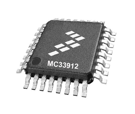
LIN system basis chip combines an SPI-controlled system basis controller with a LIN transceiver, DC motor pre-driver functions, current sensing, and protected high-side and low-side outputs. The integrated low-dropout regulator provides a 5.0 V output with 50 mA to 60 mA capability and fault reporting. The LIN interface supports LIN 2.0 and 2.1 operation, with G5 variants also supporting SAE J2602-2 conformance. The device operates from a 5.5 V to 18 V nominal supply range and supports normal, stop, and sleep operating modes with LIN and input wake-up functions. MC33912 orderable variants are supplied in a 32-pin LQFP package for -40 °C to 125 °C ambient operation.
Checking distributor stock and pricing after the page loads.
Sign in to ask questions about the NXP MC33912 datasheet using AI. Get instant answers about specifications, features, and technical details, ideal for finding information in larger documents.
Sign In to ChatWidest selection of semiconductors and electronic components in stock and ready to ship ™
| Interface | SPI-controlled LIN system basis chip |
| SPI clock frequency | Up to 4.0MHz |
| LIN data rate | Up to 100kbps |
| LIN protocol compatibility | LIN 2.0, LIN 2.1; SAE J2602-2 for G5 variants |
| Nominal supply voltage | 5.5 to 18V |
| Functional supply voltage | Up to 27V |
| Load dump voltage | Up to 40V |
| VDD regulator output voltage | 5.0 nominal, 4.75 to 5.25V |
| VDD normal-mode output current limit | 60 min, 110 typical, 200 maxmA |
| High-side switch count | 2 |
| High-side output current limit | 60 min, 90 typical, 250 maxmA |
| Low-side switch count | 2 |
| Low-side output current limit | 160 min, 275 typical, 350 maxmA |
| High-voltage inputs | 4 analog/logic inputs |
| Operating modes | Normal, Stop, Sleep |
| Ambient operating temperature, MC33912 variants | -40 to 125°C |
| Package | 32-pin LQFP |
| Pb-free | AC suffix Pb-free |
Download the complete datasheet for NXP MC33912 to view detailed technical specifications.
The embedded preview will load automatically when this section scrolls into view.
These are design resources that include the NXP MC33912
Application note for implementing a VS1 input pin filtering capacitor on NXP MC33910/11/12 SBCs to prevent resets caused by specific falling slew rate spikes.