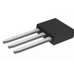
P-channel enhancement mode power MOSFET, silicon, featuring a 40V maximum drain-source voltage and 39A maximum continuous drain current. This single transistor is housed in a TO-251 (IPAK) through-hole package with 3 pins and a tab, measuring 6.55mm in length, 2.3mm in width, and 5.8mm in height. Key electrical characteristics include a ±20V maximum gate-source voltage, 3V maximum gate threshold voltage, and 18mOhm maximum drain-source resistance at 10V. The component offers typical gate charge of 27nC at 4.5V and typical input capacitance of 3000pF at 25V, with a maximum power dissipation of 1130mW.
PackageTO-251
MountingThrough Hole
Quick Jump:
Technical Specifications
Advanced Power Electronics AP9561AGJ-HF technical specifications.
General
| Package Family Name | IPAK |
| Package/Case | TO-251 |
| Package Description | Transistor Outline Package |
| Pin Count | 3 |
| PCB | 3 |
| Tab | Tab |
| Package Length (mm) | 6.55 |
| Package Width (mm) | 2.3 |
| Package Height (mm) | 5.8 |
| Pin Pitch (mm) | 2.3 |
| Package Material | Plastic |
| Mounting | Through Hole |
| Jedec | TO-251AB |
| Configuration | Single |
| Category | Power MOSFET |
| Channel Mode | Enhancement |
| Channel Type | P |
| Number of Elements per Chip | 1 |
| Maximum Drain Source Voltage | 40V |
| Maximum Gate Source Voltage | ±20V |
| Maximum Continuous Drain Current | 39A |
| Material | Si |
| Maximum Gate Threshold Voltage | 3V |
| Maximum Drain Source Resistance | 18@10VmOhm |
| Typical Gate Charge @ Vgs | [email protected]nC |
| Typical Input Capacitance @ Vds | 3000@25VpF |
| Maximum Power Dissipation | 1130mW |
| Min Operating Temperature | -55°C |
| Max Operating Temperature | 150°C |
Compliance
| EU RoHS | Yes |
| HTS Code | 8541290095 |
| Schedule B | 8541290080 |
| ECCN | EAR99 |
| RoHS Versions | 2011/65/EU, 2015/863 |
Datasheet
Advanced Power Electronics AP9561AGJ-HF Datasheet
Download the complete datasheet for Advanced Power Electronics AP9561AGJ-HF to view detailed technical specifications.
This datasheet cannot be embedded due to technical restrictions.