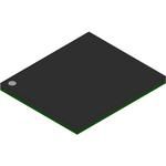
Synchronous SRAM chip, 9M-bit density, featuring a 512K x 18 configuration. Offers a 2.5 ns maximum access time and operates at a 167 MHz maximum clock rate with QDR architecture. This surface-mount component is housed in a 165-pin Fine Pitch Ball Grid Array (FBGA) package measuring 15mm x 13mm x 0.89mm. Operates from a 2.5V supply voltage, with a 2-port, pipelined architecture.
PackageFBGA
MountingSurface Mount
Quick Jump:
Technical Specifications
Cypress CY7C1302DV25-167BZXCT technical specifications.
General
| Basic Package Type | Ball Grid Array |
| Package Family Name | BGA |
| Package/Case | FBGA |
| Package Description | Fine Pitch Ball Grid Array |
| Lead Shape | Ball |
| Pin Count | 165 |
| PCB | 165 |
| Package Length (mm) | 15 |
| Package Width (mm) | 13 |
| Package Height (mm) | 0.89 |
| Seated Plane Height (mm) | 1.4(Max) |
| Pin Pitch (mm) | 1 |
| Package Weight (g) | 0.49956 |
| Package Material | Plastic |
| Mounting | Surface Mount |
| Density | 9Mbit |
| Address Bus Width | 18bit |
| Maximum Access Time | 2.5ns |
| Timing Type | Synchronous |
| Maximum Clock Rate | 167MHz |
| Data Rate Architecture | QDR |
| Density in Bits | 9437184bit |
| Maximum Operating Current | 500mA |
| Typical Operating Supply Voltage | 2.5V |
| Number of Bits per Word | 18bit |
| Number of Ports | 2 |
| Number of Words | 512K |
| Min Operating Supply Voltage | 2.4V |
| Max Operating Supply Voltage | 2.6V |
| Min Operating Temperature | 0°C |
| Max Operating Temperature | 70°C |
| Architecture | Pipelined |
Compliance
| Cage Code | 65786 |
| EU RoHS | Yes |
| HTS Code | 8542320041 |
| Schedule B | 8542320040 |
| ECCN | 3A991.b.2.a |
| Automotive | No |
| AEC Qualified | No |
| PPAP | No |
| RoHS Versions | 2011/65/EU, 2015/863 |
Datasheet
Cypress CY7C1302DV25-167BZXCT Datasheet
Download the complete datasheet for Cypress CY7C1302DV25-167BZXCT to view detailed technical specifications.
This datasheet cannot be embedded due to technical restrictions.
