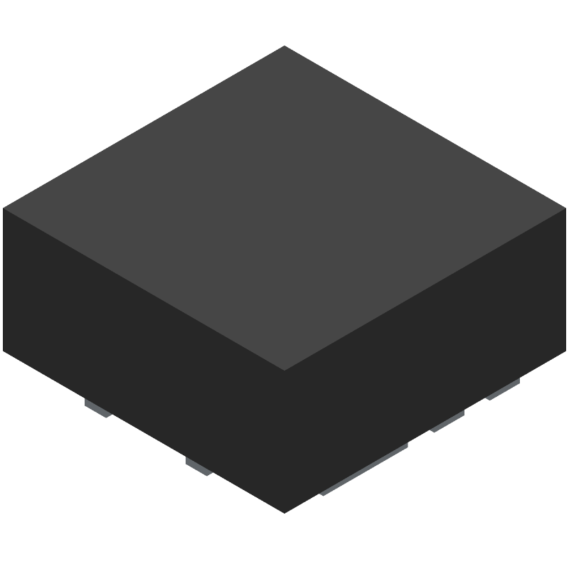
Synchronous buck power stage featuring an 8-pin SON EP package. This integrated circuit operates across a wide temperature range from -55°C to 150°C, suitable for military applications. It includes a buffer or inverter-based MOSFET driver interface, designed for a nominal supply voltage of 12V with a maximum of 22V. The component has a dual terminal position and a JEDEC package code of S-PDSO-N8, with dimensions of 3.3mm x 3.3mm.
Quick Jump:
Technical Specifications
Texas Instruments CSD86330Q3D technical specifications.
General
| Max Operating Temperature | 150 |
| Number of Terminals | 8 |
| Min Operating Temperature | -55 |
| Terminal Position | DUAL |
| JEDEC Package Code | S-PDSO-N8 |
| Width | 3.3 |
| Length | 3.3 |
| Pin Count | 8 |
| Number of Functions | 1 |
| Temperature Grade | MILITARY |
| Supply Voltage-Nom | 12 |
| Supply Voltage-Max | 22 |
| Interface IC Type | BUFFER OR INVERTER BASED MOSFET DRIVER |
| Input Characteristics | STANDARD |
Compliance
| RoHS | No |
| Eccn Code | EAR99 |
| Lead Free | Yes |
| HTS Code | 8541.29.00.95 |
| REACH | not_compliant |
| Military Spec | False |
Datasheet
Texas Instruments CSD86330Q3D Datasheet
Download the complete datasheet for Texas Instruments CSD86330Q3D to view detailed technical specifications.
This datasheet cannot be embedded due to technical restrictions.