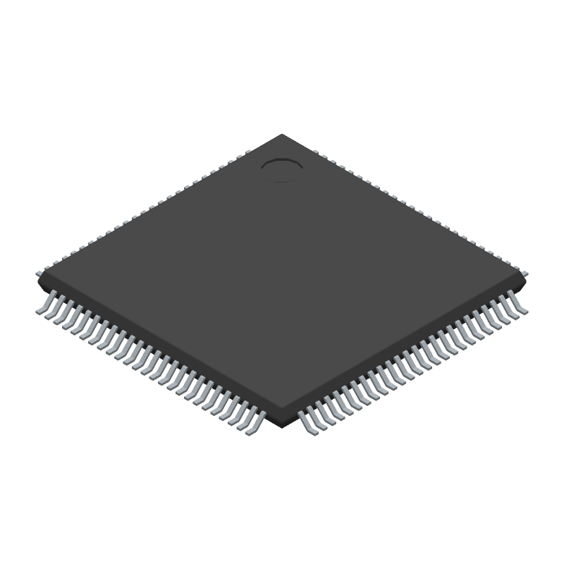
Field Programmable Gate Array (FPGA) featuring 240 Configurable Logic Blocks (CLBs) and an estimated 100,000 system gates. Operates at a maximum clock frequency of 572MHz with a 2160-cell configuration. This CMOS device is housed in a 100-terminal VQFP package (16x16mm, 1.20mm height, 0.50mm pitch). Supports a nominal supply voltage of 1.2V (1.14V to 1.26V) and offers 66 inputs and 59 outputs. Operating temperature range is 0°C to 85°C.
Quick Jump:
Technical Specifications
Xilinx XC3S100E-4VQG100C technical specifications.
General
| Max Operating Temperature | 85 |
| Number of Terminals | 100 |
| Min Operating Temperature | 0 |
| Terminal Position | QUAD |
| JEDEC Package Code | S-PQFP-G100 |
| Width | 14 |
| Length | 14 |
| Pin Count | 100 |
| Temperature Grade | OTHER |
| Supply Voltage-Nom | 1.2 |
| Supply Voltage-Min | 1.14 |
| Supply Voltage-Max | 1.26 |
| Number of Outputs | 59 |
| Clock Frequency-Max | 572 |
| Number of Inputs | 66 |
Compliance
| RoHS | Yes |
| Eccn Code | EAR99 |
| Lead Free | Yes |
| HTS Code | 8542.39.00.01 |
| REACH | Compliant |
| Military Spec | False |
Datasheet
Xilinx XC3S100E-4VQG100C Datasheet
Download the complete datasheet for Xilinx XC3S100E-4VQG100C to view detailed technical specifications.
This datasheet cannot be embedded due to technical restrictions.