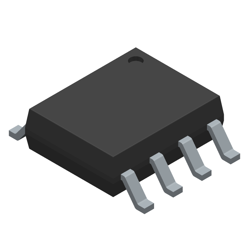
Industrial-grade PLL-based clock driver with 8 terminals in an SOIC-8 package. Features a supply voltage range of 3.15V to 3.45V, nominal 3.3V, and operates from -40°C to 85°C. Offers a maximum output current (Iol) of 0.012A and a minimum maximum frequency (fmax-Min) of 170MHz. This integrated circuit is designed for clock buffering and driving applications.
Quick Jump:
Technical Specifications
Integrated Device Technology 570BILFT technical specifications.
General
| Max Operating Temperature | 85 |
| Number of Terminals | 8 |
| Min Operating Temperature | -40 |
| Terminal Position | DUAL |
| JEDEC Package Code | R-PDSO-G8 |
| Width | 3.9 |
| Length | 4.9 |
| Pin Count | 8 |
| Number of Functions | 1 |
| Temperature Grade | INDUSTRIAL |
| Supply Voltage-Nom (Vsup) | 3.3 |
| Supply Voltage-Max (Vsup) | 3.45 |
| Supply Voltage-Min (Vsup) | 3.15 |
| Logic IC Type | PLL BASED CLOCK DRIVER |
| Family | 570 |
| Max I(ol) | 0.012 |
| fmax-Min | 170 |
Compliance
| RoHS | Yes |
| Eccn Code | EAR99 |
| Lead Free | Yes |
| HTS Code | 8542.39.00.01 |
| REACH | Compliant |
| Military Spec | False |
Datasheet
Integrated Device Technology 570BILFT Datasheet
Download the complete datasheet for Integrated Device Technology 570BILFT to view detailed technical specifications.
No datasheet is available for this part.