Lattice Semiconductor
LFE2M35SE-7FN484C
Field Programmable Gate Array, 4250 LABs, 34000 LEs, 320MHz, 1.26V
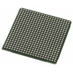
The LFE2M35SE-7FN484C is a Field Programmable Gate Array (FPGA) from Lattice Semiconductor. It features 4250 Logic Blocks (LABs) and 34000 Logic Elements/Cells. The device operates at a maximum frequency of 320MHz and is powered by a supply voltage of up to 1.26V. The FPGA is packaged in a 484-ball Flip Chip Ball Grid Array (FBGA) and is suitable for surface mount applications. The device is RoHS compliant and is available in a tray packaging with 60 units per package.
Frequency320MHz
PackageFBGA
MountingSurface Mount
Quick Jump:
Technical Specifications
Lattice Semiconductor LFE2M35SE-7FN484C technical specifications.
General
| Package/Case | FBGA |
| Lead Free | Lead Free |
| Max Frequency | 320MHz |
| Max Operating Temperature | 85°C |
| Memory Size | 2172Kb |
| Min Operating Temperature | 0°C |
| Max Supply Voltage | 1.26V |
| Min Supply Voltage | 1.14V |
| Mount | Surface Mount |
| Number of I/Os | 303 |
| Number of Logic Blocks (LABs) | 4250 |
| Number of Logic Elements/Cells | 34000 |
| Operating Supply Voltage | 1.2V |
| Package Quantity | 60 |
| Packaging | Tray |
| Radiation Hardening | No |
| RAM Size | 2151424b |
| RoHS Compliant | Yes |
| Series | ECP2M |
Compliance
| RoHS | Compliant |
Datasheet
Lattice Semiconductor LFE2M35SE-7FN484C Datasheet
Download the complete datasheet for Lattice Semiconductor LFE2M35SE-7FN484C to view detailed technical specifications.
This datasheet cannot be embedded due to technical restrictions.
Product Images
