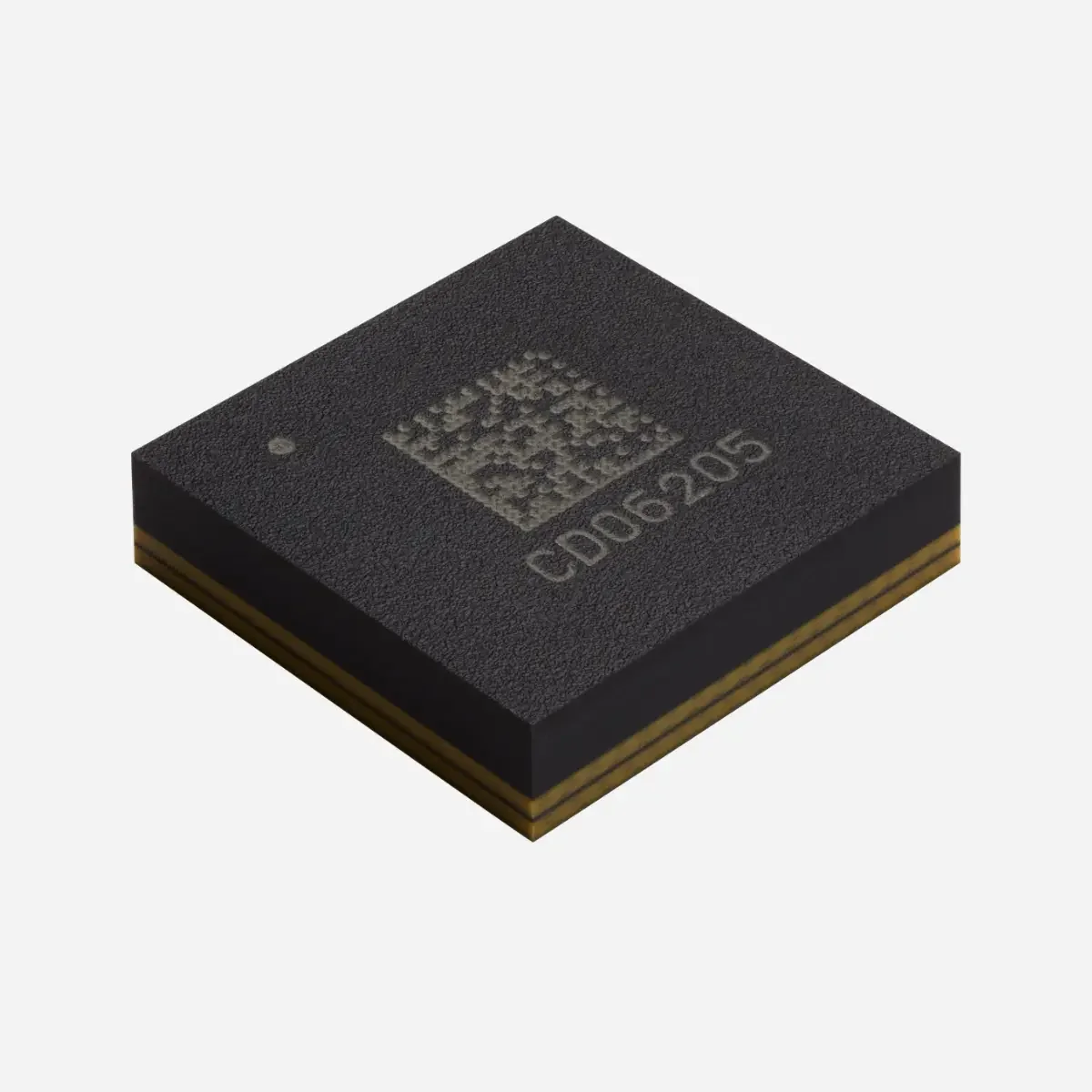
Menlo Micro's MM5625 is an Ideal Switch-based, fully integrated differential DP3T loopback module built for asymmetric SerDes test benches, delivering 80 Gbps (20 GHz) bandwidth so PCIe Gen5/Gen6 and other PAM4 links can be routed, looped back, or isolated without bulky relays. The IMS 2025 launch and the product brief detail its 12-port topology, 128 switch states, on-board charge pump/SPI control, and billions of switching cycles that drastically shorten AI/GPU validation timelines while fitting inside an 8.2 x 8.2 mm LGA SiP.
Sign in to ask questions about the Menlo Micro MM5625 datasheet using AI. Get instant answers about specifications, features, and technical details, ideal for finding information in larger documents.
Sign In to ChatWidest selection of semiconductors and electronic components in stock and ready to ship ™
Menlo Micro MM5625 technical specifications.
| Datasheet Version | v1.3 |
| Operating Frequency Range | DC to 20GHz |
| Switch Type | Differential Dual DP3T with Loopback |
| Actuator Type | Normally Open, Reflective |
| Insertion Loss (Typical) | -2.7dB @ 20 GHz |
| Integrated Features | Charge Pump and Driver, AC Coupling Capacitors |
| Signal Routing Control | Fully controllable ports |
| Switching Cycles (Minimum) | 3 billioncycles |
| Package Type | LGA8.2 x 8.2 mm |
| Control States | 128 |
| Absolute Max DC Supply Voltage (VDD) | -0.3 to 3.6V |
| Absolute Max I/O Supply Voltage (VDD_IO) | -0.3 to 5.5V |
| Absolute Max Charge Pump Input (VIN) | -0.3 to 5.5V |
| Absolute Max Driver Logic Input Levels | -0.3 to VDD_IO + 0.3V |
| Absolute Max RF Pin Input Voltage | 3.3V |
| Absolute Max Hot Switching Voltage | -0.5 to 0.5V |
| Absolute Max Storage Temperature | -65 to 150°C |
| Absolute Max ESD HBM RF Pins | 150V |
| Absolute Max ESD HBM Control/Power Pins | 2000V |
| Absolute Max ESD HBM VPP Pin | 500V |
| Absolute Max Mechanical Shock | 500G |
| Absolute Max Vibration | 500Hz |
| Absolute Max RF Input Power | 20dBm into 50 ohms |
| Recommended Charge Pump Power Supply (VIN) | 4.75 to 5.5V |
| Recommended Driver Logic Supply Voltage (VDD) | 3.0 to 3.6V |
| Recommended Logic Reference Level (VDD_IO) | 1.71 to 5.25V |
| Recommended Operating Temperature | -40 to 85°C Ambient |
| Recommended Switch Cycle Frequency | 100Hz |
| Differential Insertion Loss (HS1 to HS2) Typical | 2.7dB @ 20GHz |
| Differential Insertion Loss (MS1 to MS2) Typical | 2.2dB @ 16GHz |
| Differential Return Loss (HS1 to HS2) Typical | 18dB @ 20GHz |
| Differential Isolation (HS1 to HS2) Typical | 46dB @ 20GHz |
| PAM4 Eye Diagram Bit Rate | 80Gbps |
| PAM4 Eye Height (0/1) | 79.74mV @ 80 Gbps |
| PAM4 Eye Width (0/1) | 10.54ps @ 80 Gbps |
| PAM4 Total Jitter (0/1) | 7.23ps RMS @ 80 Gbps |
| Switch Settling Time (On) Typical | 26.5µs |
| Switch Settling Time (Off) Typical | 9µs |
| On-State Resistance (RON) Typical | 1.7Ω |
| On-State Resistance (RON) Maximum | 4.0Ω |
| Off-State Leakage Current (Typical) | 7nA @ 30VDC |
| Off-State Leakage Current (Maximum) | 60nA @ 30VDC |
| Charge Pump Power Supply (VIN) Typical | 5.0V |
| Charge Pump Power Supply (VIN) Minimum | 4.75V |
| Charge Pump Power Supply (VIN) Maximum | 5.5V |
| VIN Current (Dynamic) Typical | 1.7mA |
| VIN Current (Dynamic) Maximum | 2.75mA |
| VIN Quiescent Current Typical | 1.65mA |
| VIN Quiescent Current Maximum | 2.25mA |
| Low Voltage Logic Supply (VDD) Typical | 3.3V |
| Low Voltage Logic Supply (VDD) Minimum | 3.0V |
| Low Voltage Logic Supply (VDD) Maximum | 3.6V |
| VDD UVLO Rising Threshold Typical | 2.77V |
| VDD UVLO Rising Threshold Maximum | 2.95V |
| VDD UVLO Falling Threshold Typical | 2.72V |
| VDD UVLO Falling Threshold Maximum | 2.90V |
| Low Voltage Digital Current Typical | 520µA |
| Low Voltage Digital Current Maximum | 700µA |
| Low Voltage Digital Quiescent Current Typical | 480µA |
| Low Voltage Digital Quiescent Current Maximum | 550µA |
| Low Voltage Digital Sleep Mode Current Typical | <1µA |
| Low Voltage Digital Sleep Mode Current Maximum | 10µA |
| Logic Reference Level (VDD_IO) Minimum | 1.71V |
| Logic Reference Level (VDD_IO) Maximum | 5.25V |
| I/O Logic Supply Current Typical | <10µA |
| I/O Logic Supply Current Maximum | 50µA |
| SPI Clock Frequency (Max) | 33MHz |
| SDI Valid to SCK Setup Time (Min) | 2ns |
| SDI Valid to SCK Hold Time (Min) | 5ns |
| SCK High Time (Min) | 15.5ns |
| SCK Low Time (Min) | 15.5ns |
| SSB Pulse Width (Min) | 15ns |
| LSB SCK to SSB High (Min) | 15ns |
| SSB Low to SCK High (Min) | 15ns |
| SDO Propagation Delay from SCK Falling Edge (Max) | 10ns |
| SDO Output Valid after SSB Low (Typical) | 20ns |
| SSB Inactive to SDO High Impedance (Max) | 10ns |
| Power-On-Reset Time (Typical) | 1.25ms |
| Power-On-Reset Time (Maximum) | 2.5ms |
| Start-Up Time (Typical) | 20ms |
| Start-Up Time (Maximum) | 33ms |
| Operating Current (IVIND) | 1.7 (typical), 2.75 (max)mA |
| RoHS | Compliant |
| Ear | EAR99 |
Download the complete datasheet for Menlo Micro MM5625 to view detailed technical specifications.
The embedded preview will load automatically when this section scrolls into view.