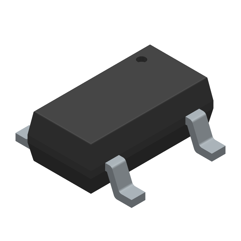
Automotive-grade bus driver with 3-state output, featuring a single 1-bit buffer function. Operates with a supply voltage range of 1.65V to 5.5V, nominal 3.3V, and offers a propagation delay of 10.5ns. This TSOP 5-pin device, with a JEDEC package code of R-PDSO-G5, measures 1.5mm in width and 2.9mm in length, supporting dual terminal positions. Designed for operation between -40°C and 125°C.
Quick Jump:
Technical Specifications
Nexperia 74LVC1G125GV,125 technical specifications.
General
| Max Operating Temperature | 125 |
| Number of Terminals | 5 |
| Min Operating Temperature | -40 |
| Terminal Position | DUAL |
| JEDEC Package Code | R-PDSO-G5 |
| Width | 1.5 |
| Length | 2.9 |
| Pin Count | 5 |
| Number of Functions | 1 |
| Temperature Grade | AUTOMOTIVE |
| Supply Voltage-Nom (Vsup) | 3.3 |
| Supply Voltage-Max (Vsup) | 5.5 |
| Supply Voltage-Min (Vsup) | 1.65 |
| Logic IC Type | BUS DRIVER |
| Family | LVC/LCX/Z |
| Propagation Delay (tpd) | 10.5 |
| Number of Bits | 1 |
| Output Polarity | TRUE |
| Number of Ports | 2 |
Compliance
| HTS Code | 8542.39.00.01 |
| REACH | Compliant |
| Military Spec | False |
Datasheet
Nexperia 74LVC1G125GV,125 Datasheet
Download the complete datasheet for Nexperia 74LVC1G125GV,125 to view detailed technical specifications.
This datasheet cannot be embedded due to technical restrictions.