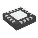
1:1 Clock Multiplexer, featuring 1 LVDS output and supporting LVCMOS, LVDS, LVPECL, and LVTTL inputs. Operates with a maximum input frequency of 2500 MHz, a supply voltage range of 3.135V to 3.465V, and an operating temperature range of -40°C to 85°C. Housed in a 16-pin VFQFPN EP package with a 0.5mm pin pitch, measuring 3.1mm x 3.1mm x 1mm. Surface mountable, this component is designed for high-speed clock distribution applications.
PackageVFQFPN EP
MountingSurface Mount
Quick Jump:
Technical Specifications
Renesas 854S01AKILF technical specifications.
General
| Basic Package Type | Non-Lead-Frame SMT |
| Package Family Name | QFN |
| Package/Case | VFQFPN EP |
| Package Description | Very Fine Quad Flat Package No Lead, Exposed Pad |
| Lead Shape | No Lead |
| Pin Count | 16 |
| PCB | 16 |
| Package Length (mm) | 3.1(Max) |
| Package Width (mm) | 3.1(Max) |
| Package Height (mm) | 1(Max) |
| Seated Plane Height (mm) | 1.05(Max) |
| Pin Pitch (mm) | 0.5 |
| Package Material | Plastic |
| Mounting | Surface Mount |
| Jedec | MO-220 |
| Type | Clock Multiplexer |
| Number of Outputs per Chip | 1 |
| Output Logic Level | LVDS |
| Input Logic Level | LVCMOS|LVDS|LVPECL|LVTTL |
| Maximum Input Frequency | 2500MHz |
| Min Operating Supply Voltage | 3.135V |
| Max Operating Supply Voltage | 3.465V |
| Min Operating Temperature | -40°C |
| Max Operating Temperature | 85°C |
Compliance
| Cage Code | SAN34 |
| EU RoHS | Yes |
| HTS Code | 8542390001 |
| Schedule B | 8542390000 |
| ECCN | EAR99 |
| Automotive | No |
| AEC Qualified | No |
| PPAP | No |
| Radiation Hardening | No |
| RoHS Versions | 2011/65/EU, 2015/863 |
Datasheet
Renesas 854S01AKILF Datasheet
Download the complete datasheet for Renesas 854S01AKILF to view detailed technical specifications.
This datasheet cannot be embedded due to technical restrictions.