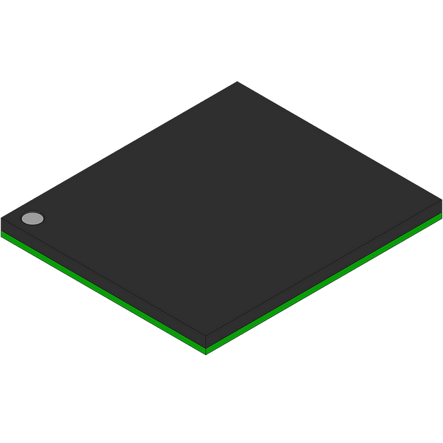
2MX18 DDR SRAM with a 0.45ns access time and 250MHz maximum clock frequency. This parallel interface memory features a pipelined architecture and a 2M x 18 organization. Operating from 1.7V to 1.9V, it offers separate I/O and 3-state output characteristics. Housed in a 165-ball PBGA package measuring 15mm x 17mm with a 1mm terminal pitch, this surface-mount component is designed for commercial temperature ranges.
Quick Jump:
Technical Specifications
Renesas UPD44324185BF5-E40-FQ1 technical specifications.
General
| Access Time-Max | 0.45ns |
| Additional Feature | PIPELINED ARCHITECTURE |
| Clock Frequency-Max (fCLK) | 250MHz |
| Density | 37748736b |
| Height - Seated (Max) | 1.46mm |
| I/O Type | SEPARATE |
| JESD-30 Code | R-PBGA-B165 |
| Length | 17mm |
| Max Operating Temperature | 70°C |
| Min Operating Temperature | 0°C |
| Max Supply Current | 480mA |
| Memory Type | DDR SRAM |
| Memory Width | 18 |
| Number of Functions | 1 |
| Number of Words | 2097152 |
| Number of Words Code | 2M |
| Organization | 2MX18 |
| Output Characteristics | 3-STATE |
| Package Body Material | Plastic |
| Package Code | LBGA |
| Package Equivalence Code | BGA165,11X15,40 |
| Package Shape | Rectangular |
| Package Style | GRID ARRAY, LOW PROFILEMeter |
| Parallel/Serial | PARALLEL |
| Power Supplies | 1.5/1.8,1.8V |
| Qualification Status | Not Qualified |
| RoHS Compliant | No |
| Standby Current-Max | 380mA |
| Standby Voltage-Min | 1.7V |
| Supply Voltage-Max (Vsup) | 1.9V |
| Supply Voltage-Min (Vsup) | 1.7V |
| Supply Voltage-Nom (Vsup) | 1.8V |
| Surface Mount | Yes |
| Technology | CMOS |
| Temperature Grade | COMMERCIAL |
| Terminal Form | Ball |
| Terminal Pitch | 1mm |
| Terminal Position | BOTTOM |
| Width | 15mm |
Compliance
| RoHS | Not Compliant |
Datasheet
Renesas UPD44324185BF5-E40-FQ1 Datasheet
Download the complete datasheet for Renesas UPD44324185BF5-E40-FQ1 to view detailed technical specifications.
This datasheet cannot be embedded due to technical restrictions.
Product Images

