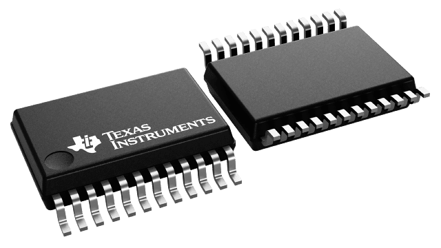
10-output, 1-input clock buffer and driver IC, operating at 3.3V with a maximum frequency of 100MHz. Features tri-state outputs, LVTTL input compatibility, and a propagation delay of 6.4ns. Packaged in a 24-pin SOIC with gold contact plating, suitable for surface mounting. Operates across a temperature range of -40°C to 85°C with a supply voltage range of 3V to 3.6V. RoHS compliant and lead-free.
Frequency100MHz
PackageSOIC
MountingSurface Mount
Power1.7W
Quick Jump:
Technical Specifications
Texas Instruments CDC351DWR technical specifications.
General
| Package/Case | SOIC |
| Contact Plating | Gold |
| Frequency | 100MHz |
| Input | LVTTL |
| Lead Free | Lead Free |
| Max Frequency | 100MHz |
| Max Operating Temperature | 85°C |
| Min Operating Temperature | -40°C |
| Max Supply Voltage | 3.6V |
| Min Supply Voltage | 3V |
| Mount | Surface Mount |
| Nominal Supply Current | 25mA |
| Number of Circuits | 1 |
| Number of Outputs | 10 |
| Operating Supply Voltage | 3.3V |
| Package Quantity | 2000 |
| Packaging | Tape and Reel |
| Power Dissipation | 1.7W |
| Propagation Delay | 6.4ns |
| Quiescent Current | 25mA |
| Radiation Hardening | No |
| RoHS Compliant | Yes |
| Series | CDC351 |
| Turn-On Delay Time | 6.4ns |
| Weight | 0.022025oz |
Compliance
| RoHS | Compliant |
Datasheet
Texas Instruments CDC351DWR Datasheet
Download the complete datasheet for Texas Instruments CDC351DWR to view detailed technical specifications.
This datasheet cannot be embedded due to technical restrictions.
