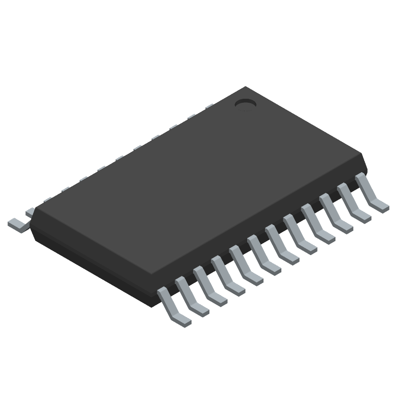
The CDCLVC1112PW is an industrial-grade clock driver IC with 24 terminals, operating within a temperature range of -40 to 85 degrees Celsius. It has a nominal supply voltage of 2.5V and a maximum supply voltage of 2.7V. The device features a low skew clock driver with a propagation delay of 2.6ns and a maximum output current of 12uA. It is packaged in a TSSOP-24 package with a width of 4.4mm and a length of 7.8mm.
Quick Jump:
Technical Specifications
Texas Instruments CDCLVC1112PW technical specifications.
General
| Max Operating Temperature | 85 |
| Number of Terminals | 24 |
| Min Operating Temperature | -40 |
| Terminal Position | DUAL |
| JEDEC Package Code | R-PDSO-G24 |
| Width | 4.4 |
| Length | 7.8 |
| Pin Count | 24 |
| Number of Functions | 1 |
| Temperature Grade | INDUSTRIAL |
| Supply Voltage-Nom (Vsup) | 2.5 |
| Supply Voltage-Max (Vsup) | 2.7 |
| Supply Voltage-Min (Vsup) | 2.3 |
| Logic IC Type | LOW SKEW CLOCK DRIVER |
| Family | CDC |
| Propagation Delay (tpd) | 2.6 |
| Max I(ol) | 0.012 |
| Prop. Delay@Nom-Sup | 2 |
| fmax-Min | 250 |
Compliance
| RoHS | Yes |
| Eccn Code | EAR99 |
| Lead Free | Yes |
| HTS Code | 8542.39.00.01 |
| REACH | Compliant |
| Military Spec | False |
Datasheet
Texas Instruments CDCLVC1112PW Datasheet
Download the complete datasheet for Texas Instruments CDCLVC1112PW to view detailed technical specifications.
This datasheet cannot be embedded due to technical restrictions.