P-Channel NexFET™ Power MOSFET featuring a 20V Drain to Source Breakdown Voltage and 75mΩ Drain to Source Resistance. Continuous Drain Current (ID) is 2.2A with a maximum power dissipation of 1.5W. Operating temperature range spans from -55°C to 150°C. Surface mountable in a 6-DSBGA package, it offers fast switching with a 4ns turn-on delay and 12ns fall time. Contact plating includes Copper, Tin, and Silver.
MountingSurface Mount
PolarityP-CHANNEL
Power1.5W
Quick Jump:
Technical Specifications
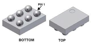
Texas Instruments CSD25301W1015 technical specifications.
General
| Contact Plating | Copper, Tin, Silver |
| Continuous Drain Current (ID) | 2.2A |
| Drain to Source Breakdown Voltage | 20V |
| Drain to Source Resistance | 75mR |
| Drain to Source Voltage (Vdss) | 20V |
| Dual Supply Voltage | 20V |
| Fall Time | 12ns |
| Gate to Source Voltage (Vgs) | 8V |
| Input Capacitance | 270pF |
| Lead Free | Contains Lead |
| Max Operating Temperature | 150°C |
| Min Operating Temperature | -55°C |
| Max Power Dissipation | 1.5W |
| Mount | Surface Mount |
| Nominal Vgs | 750mV |
| Package Quantity | 3000 |
| Packaging | Tape and Reel |
| Polarity | P-CHANNEL |
| Power Dissipation | 1.5W |
| Rds On Max | 75mR |
| Reach SVHC Compliant | No |
| RoHS Compliant | Yes |
| Series | NexFET™ |
| Termination | SMD/SMT |
| Turn-Off Delay Time | 29ns |
| Turn-On Delay Time | 4ns |
Compliance
| RoHS | Compliant |
Datasheet
Texas Instruments CSD25301W1015 Datasheet
Download the complete datasheet for Texas Instruments CSD25301W1015 to view detailed technical specifications.
This datasheet cannot be embedded due to technical restrictions.
Product Images