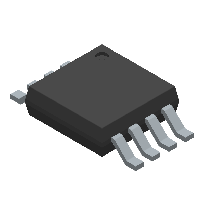
Dual, nanopower operational amplifier featuring CMOS inputs and Rail-to-Rail Input/Output (RRIO) operation. This voltage-feedback amplifier offers a nominal supply voltage of 3.3V with a maximum limit of 6V, and a maximum supply current of 1.6µA. Key specifications include a minimum voltage gain of 35481, a nominal slew rate of 0.0037V/µs, and a unity gain bandwidth of 8MHz. Designed for cost-sensitive automotive applications, it operates across a temperature range of -40°C to 125°C and is AEC-Q100 screened. The 8-terminal S-PDSO-G8 package measures 3mm x 3mm.
Sign in to ask questions about the Texas Instruments TLV522DGKR datasheet using AI. Get instant answers about specifications, features, and technical details, ideal for finding information in larger documents.
Sign In to ChatWidest selection of semiconductors and electronic components in stock and ready to ship ™
Texas Instruments TLV522DGKR technical specifications.
| Max Operating Temperature | 125 |
| Number of Terminals | 8 |
| Min Operating Temperature | -40 |
| Terminal Position | DUAL |
| JEDEC Package Code | S-PDSO-G8 |
| Width | 3 |
| Length | 3 |
| Number of Functions | 2 |
| Temperature Grade | AUTOMOTIVE |
| Supply Voltage-Nom (Vsup) | 3.3 |
| Supply Current-Max | 0.0016 |
| Amplifier Type | OPERATIONAL AMPLIFIER |
| Supply Voltage Limit-Max | 6 |
| Input Offset Voltage-Max | 4000 |
| Architecture | VOLTAGE-FEEDBACK |
| Slew Rate-Nom | 0.0037 |
| Frequency Compensation | YES |
| Low-Offset | NO |
| Common-mode Reject Ratio-Nom | 90 |
| Voltage Gain-Min | 35481 |
| Unity Gain BW-Nom | 8 |
| Low-Bias | YES |
| Micropower | YES |
| Screening Level | AEC-Q100 |
| RoHS | Yes |
| Lead Free | Yes |
| REACH | Compliant |
| Military Spec | False |
Download the complete datasheet for Texas Instruments TLV522DGKR to view detailed technical specifications.
The embedded preview will load automatically when this section scrolls into view.