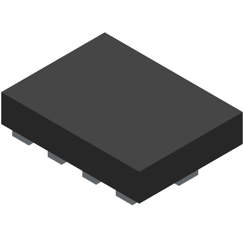
Dual-channel, 10-MHz operational amplifier featuring Rail-to-Rail Input/Output (RRIO) and CMOS technology. This automotive-grade amplifier offers a 1.5mm width, 2mm length, 10-terminal JEDEC R-PQCC-N10 package, and operates from -40°C to 125°C. Key specifications include a nominal supply voltage of 5V (up to 6V limit), 1.5mA maximum supply current, 1600µV maximum input offset voltage, 500nA maximum average bias current, and a 6.5V/µs nominal slew rate. Achieves 103dB nominal common-mode reject ratio and 10MHz nominal unity gain bandwidth.
Quick Jump:
Technical Specifications
Texas Instruments TLV9062SIRUGR technical specifications.
General
| Max Operating Temperature | 125 |
| Number of Terminals | 10 |
| Min Operating Temperature | -40 |
| Terminal Position | QUAD |
| JEDEC Package Code | R-PQCC-N10 |
| Width | 1.5 |
| Length | 2 |
| Number of Functions | 2 |
| Temperature Grade | AUTOMOTIVE |
| Supply Voltage-Nom (Vsup) | 5 |
| Supply Current-Max | 1.5 |
| Amplifier Type | OPERATIONAL AMPLIFIER |
| Supply Voltage Limit-Max | 6 |
| Input Offset Voltage-Max | 1600 |
| Average Bias Current-Max (IIB) | 5e-7 |
| Slew Rate-Nom | 6.5 |
| Common-mode Reject Ratio-Nom | 103 |
| Unity Gain BW-Nom | 10000 |
Compliance
| RoHS | Yes |
| Lead Free | Yes |
| REACH | Compliant |
| Military Spec | False |
Datasheet
Texas Instruments TLV9062SIRUGR Datasheet
Download the complete datasheet for Texas Instruments TLV9062SIRUGR to view detailed technical specifications.
This datasheet cannot be embedded due to technical restrictions.