N-channel enhancement mode power MOSFET featuring a 900V maximum drain-source voltage and 1A continuous drain current. This single-element silicon transistor is housed in a 3-pin (2+Tab) Case DP surface-mount package with a maximum package height of 2.5mm. Key electrical characteristics include a maximum drain-source resistance of 9000 mOhm at 10V and a typical gate charge of 15 nC at 10V. Operating temperature range spans from -55°C to 150°C, with a maximum power dissipation of 40000 mW.
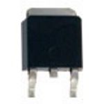
PackageCase DP
MountingSurface Mount
Quick Jump:
Technical Specifications
Toshiba 2SK2845(PP) technical specifications.
General
| Package/Case | Case DP |
| Pin Count | 3 |
| PCB | 2 |
| Tab | Tab |
| Package Length (mm) | 6.8(Max) |
| Package Width (mm) | 5.5 |
| Package Height (mm) | 2.5(Max) |
| Seated Plane Height (mm) | 2.7(Max) |
| Mounting | Surface Mount |
| Configuration | Single |
| Category | Power MOSFET |
| Channel Mode | Enhancement |
| Channel Type | N |
| Number of Elements per Chip | 1 |
| Maximum Drain Source Voltage | 900V |
| Maximum Gate Source Voltage | ±30V |
| Maximum Continuous Drain Current | 1A |
| Material | Si |
| Maximum Drain Source Resistance | 9000@10VmOhm |
| Typical Gate Charge @ Vgs | 15@10VnC |
| Typical Gate Charge @ 10V | 15nC |
| Typical Input Capacitance @ Vds | 350@25VpF |
| Maximum Power Dissipation | 40000mW |
| Min Operating Temperature | -55°C |
| Max Operating Temperature | 150°C |
Compliance
| Cage Code | S0562 |
| HTS Code | 8541290095 |
| Schedule B | 8541290080 |
| ECCN | EAR99 |
| Automotive | No |
| AEC Qualified | No |
| PPAP | No |
| Radiation Hardening | No |
| RoHS Versions | 2002/95/EC |
Datasheet
Toshiba 2SK2845(PP) Datasheet
Download the complete datasheet for Toshiba 2SK2845(PP) to view detailed technical specifications.
This datasheet cannot be embedded due to technical restrictions.