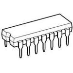
Quad low-power operational amplifier featuring BiFET process technology. This through-hole mounted IC offers four independent amplifier channels within a 14-pin PDIP package. It operates with dual supply voltages ranging from ±2V to ±18V, supporting typical dual supplies of ±3V, ±5V, ±9V, ±12V, and ±15V. Maximum input offset voltage is 15mV at ±15V, with a maximum input bias current of 0.0004µA at ±15V. Operating temperature range is -40°C to 85°C.
PackagePDIP
MountingThrough Hole
Quick Jump:
Technical Specifications
Toshiba TA75064P(J) technical specifications.
General
| Basic Package Type | Through Hole |
| Package Family Name | DIP |
| Package/Case | PDIP |
| Package Description | Plastic Dual In Line Package |
| Lead Shape | Through Hole |
| Pin Count | 14 |
| PCB | 14 |
| Package Length (mm) | 19.75(Max) |
| Package Width (mm) | 6.4 |
| Package Height (mm) | 3.5 |
| Seated Plane Height (mm) | 4.15 |
| Pin Pitch (mm) | 2.54 |
| Package Weight (g) | 0.96 |
| Package Material | Plastic |
| Mounting | Through Hole |
| Jedec | MS-001AA |
| Manufacturer Type | Low Power Amplifier |
| Type | Low Power Amplifier |
| Number of Channels per Chip | 4 |
| Process Technology | BiFET |
| Maximum Input Offset Voltage | 15@±15VmV |
| Maximum Input Offset Current | 0.0002@±15VuA |
| Maximum Input Bias Current | 0.0004@±15VuA |
| Min Operating Temperature | -40°C |
| Max Operating Temperature | 85°C |
| Minimum Dual Supply Voltage | ±2V |
| Maximum Dual Supply Voltage | ±18V |
| Typical Dual Supply Voltage | ±3|±5|±9|±12|±15V |
| Maximum Supply Voltage Range | 36 to 37V |
| Max Operating Supply Voltage | ±18V |
Compliance
| Cage Code | S0562 |
| HTS Code | 8542330001 |
| Schedule B | 8542330000 |
| ECCN | EAR99 |
| Automotive | No |
| AEC Qualified | No |
| PPAP | No |
| Radiation Hardening | No |
Datasheet
Toshiba TA75064P(J) Datasheet
Download the complete datasheet for Toshiba TA75064P(J) to view detailed technical specifications.
This datasheet cannot be embedded due to technical restrictions.