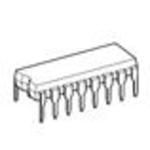
NPN bipolar junction transistor array featuring 7 elements in a 16-pin PDIP through-hole package. This silicon component offers a maximum collector-emitter voltage of 35V and a maximum DC collector current of 0.2A. With a minimum DC current gain of 70 at 10mA and 10V, it is suitable for applications requiring up to 1000mW of power dissipation. The package dimensions are 19.75mm (max) length, 6.4mm width, and 3.5mm height, with a 2.54mm pin pitch. Operating temperature range is -40°C to 85°C.
PackagePDIP
MountingThrough Hole
Quick Jump:
Technical Specifications
Toshiba TD62501P(J) technical specifications.
General
| Basic Package Type | Through Hole |
| Package Family Name | DIP |
| Package/Case | PDIP |
| Package Description | Plastic Dual In Line Package |
| Lead Shape | Through Hole |
| Pin Count | 16 |
| PCB | 16 |
| Package Length (mm) | 19.75(Max) |
| Package Width (mm) | 6.4 |
| Package Height (mm) | 3.5 |
| Seated Plane Height (mm) | 4.15 |
| Pin Pitch (mm) | 2.54 |
| Package Material | Plastic |
| Mounting | Through Hole |
| Jedec | MS-001BB |
| Type | NPN |
| Configuration | Array 7 |
| Number of Elements per Chip | 7 |
| Maximum Collector Base Voltage | 50V |
| Maximum Collector-Emitter Voltage | 35V |
| Maximum DC Collector Current | 0.2A |
| Maximum Power Dissipation | 1000mW |
| Material | Si |
| Minimum DC Current Gain | 70@10mA@10V |
| Category | Bipolar Power |
| Min Operating Temperature | -40°C |
| Max Operating Temperature | 85°C |
Compliance
| Cage Code | S0562 |
| Schedule B | 8541290080 |
| ECCN | EAR99 |
| Automotive | No |
| AEC Qualified | No |
| PPAP | No |
| Radiation Hardening | No |
Datasheet
Toshiba TD62501P(J) Datasheet
Download the complete datasheet for Toshiba TD62501P(J) to view detailed technical specifications.
This datasheet cannot be embedded due to technical restrictions.