N-channel enhancement mode power MOSFET, silicon, featuring 100V drain-source voltage and 75A continuous drain current. This single element transistor utilizes U-MOS VIII-H process technology and is housed in a TO-220SIS package with 3 pins and a tab, suitable for through-hole mounting. Key specifications include a maximum gate-source voltage of ±20V, a low drain-source on-resistance of 9.5mΩ at 10V, and a typical gate charge of 38nC at 10V. Maximum power dissipation is 35000mW, with an operating temperature range of -55°C to 150°C.
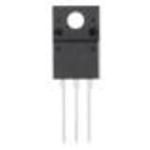
PackageTO-220SIS
MountingThrough Hole
Quick Jump:
Technical Specifications
Toshiba TK34A10N1 technical specifications.
General
| Basic Package Type | Through Hole |
| Package Family Name | TO-220 |
| Package/Case | TO-220SIS |
| Pin Count | 3 |
| PCB | 3 |
| Tab | Tab |
| Package Length (mm) | 10 |
| Package Width (mm) | 4.5 |
| Package Height (mm) | 15 |
| Seated Plane Height (mm) | 17 |
| Pin Pitch (mm) | 2.54 |
| Package Material | Plastic |
| Mounting | Through Hole |
| Configuration | Single |
| Category | Power MOSFET |
| Channel Mode | Enhancement |
| Channel Type | N |
| Number of Elements per Chip | 1 |
| Process Technology | U-MOS VIII-H |
| Maximum Drain Source Voltage | 100V |
| Maximum Gate Source Voltage | ±20V |
| Maximum Continuous Drain Current | 75A |
| Material | Si |
| Maximum Gate Threshold Voltage | 4V |
| Maximum Drain Source Resistance | 9.5@10VmOhm |
| Typical Gate Charge @ Vgs | 38@10VnC |
| Typical Gate Charge @ 10V | 38nC |
| Typical Input Capacitance @ Vds | 2600@50VpF |
| Maximum Power Dissipation | 35000mW |
| Min Operating Temperature | -55°C |
| Max Operating Temperature | 150°C |
Compliance
| Cage Code | S0562 |
| EU RoHS | Yes |
| HTS Code | 8541290095 |
| Schedule B | 8541290080 |
| ECCN | EAR99 |
| Automotive | No |
| AEC Qualified | No |
| PPAP | No |
| RoHS Versions | 2011/65/EU |
Datasheet
Toshiba TK34A10N1 Datasheet
Download the complete datasheet for Toshiba TK34A10N1 to view detailed technical specifications.
This datasheet cannot be embedded due to technical restrictions.