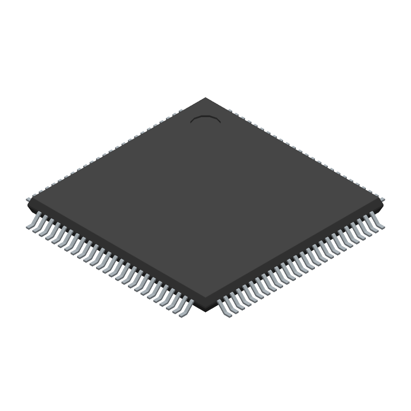
High-performance Field Programmable Gate Array (FPGA) featuring 176 Configurable Logic Blocks (CLBs) and 50,000 system gates. Operates at a maximum clock frequency of 667 MHz, with 1584 logic cells. This CMOS device utilizes a 100-terminal Quad Flat Package (QFP) with a 1.20 mm height and 0.50 mm pitch, measuring 14 x 14 mm. Designed for industrial temperature ranges from -40°C to 100°C, with a nominal supply voltage of 1.2V. Includes 62 outputs and 68 inputs.
Checking distributor stock and pricing after the page loads.
Sign in to ask questions about the Xilinx XC3S50A-4VQG100I datasheet using AI. Get instant answers about specifications, features, and technical details, ideal for finding information in larger documents.
Sign In to ChatWidest selection of semiconductors and electronic components in stock and ready to ship ™
| Max Operating Temperature | 100 |
| Number of Terminals | 100 |
| Min Operating Temperature | -40 |
| Terminal Position | QUAD |
| JEDEC Package Code | S-PQFP-G100 |
| Width | 14 |
| Length | 14 |
| Pin Count | 100 |
| Temperature Grade | INDUSTRIAL |
| Supply Voltage-Nom | 1.2 |
| Supply Voltage-Min | 1.14 |
| Supply Voltage-Max | 1.26 |
| Number of Outputs | 62 |
| Clock Frequency-Max | 667 |
| Number of Inputs | 68 |
| RoHS | Yes |
| Eccn Code | EAR99 |
| HTS Code | 8542.39.00.01 |
| REACH | Compliant |
| Military Spec | False |
Download the complete datasheet for Xilinx XC3S50A-4VQG100I to view detailed technical specifications.
The embedded preview will load automatically when this section scrolls into view.