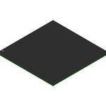
Lidless FCBGA Flip Chip Ball Grid Array FPGA with 676 pins, 27mm x 27mm x 1.84mm dimensions and 1mm pin pitch. Features 125,000 logic cells, 157,200 registers, 1060 Kbit RAM, and 400 dedicated DSP slices. Supports 128 user I/Os, 2 Ethernet MACs, and 400 multipliers (18x25). Operates across a -40°C to 100°C temperature range.
PackageLidless FCBGA
MountingSurface Mount
Quick Jump:
Technical Specifications
Xilinx XC7Z030-2FBG676I technical specifications.
General
| Basic Package Type | Ball Grid Array |
| Package Family Name | Lidless FCBGA |
| Package/Case | Lidless FCBGA |
| Package Description | Flip Chip Lidless Ball Grid Array |
| Lead Shape | Ball |
| Pin Count | 676 |
| PCB | 676 |
| Package Length (mm) | 27 |
| Package Width (mm) | 27 |
| Package Height (mm) | 1.84 |
| Seated Plane Height (mm) | 2.34 |
| Pin Pitch (mm) | 1 |
| Package Material | Plastic |
| Mounting | Surface Mount |
| Family Name | Kintex-7 |
| Maximum Number of User I/Os | 128 |
| Number of Registers | 157200 |
| RAM Bits | 1060Kbit |
| Device Logic Cells | 125000 |
| Process Technology | 28nm |
| Ethernet MACs | 2 |
| Number of Multipliers | 400 (18x25) |
| Programmability | Yes |
| Program Memory Type | SRAM |
| Min Operating Temperature | -40°C |
| Max Operating Temperature | 100°C |
| Dedicated DSP | 400 |
| Speed Grade | 2 |
| Differential I/O Standards Supported | LVDS|SSTL|HSTL |
| Device Number of DLLs/PLLs | 5 |
| Total Number of Block RAM | 265 |
Compliance
| Cage Code | 68994 |
| EU RoHS | Yes |
| HTS Code | 8542390001 |
| Schedule B | 8542390000 |
| ECCN | 3A991.d |
| Automotive | Yes |
| RoHS Versions | 2011/65/EU, 2015/863 |
Datasheet
Xilinx XC7Z030-2FBG676I Datasheet
Download the complete datasheet for Xilinx XC7Z030-2FBG676I to view detailed technical specifications.
This datasheet cannot be embedded due to technical restrictions.
