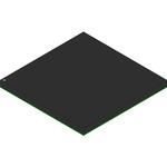
Field Programmable Gate Array (FPGA) with 125,000 logic cells and 157,200 registers, built on 28nm process technology. This device features 1060 Kbit of RAM, 400 multipliers (18x25), and 400 dedicated DSP slices. It supports 2 Ethernet MACs and offers 5 DLLs/PLLs, with a total of 265 Block RAMs. The 676-pin Fine Pitch Ball Grid Array (FCBGA) package, measuring 27x27mm with a 1mm pin pitch, is designed for surface mounting and operates within a -40°C to 100°C temperature range.
PackageFCBGA
MountingSurface Mount
Quick Jump:
Technical Specifications
Xilinx XC7Z030-2FFG676I technical specifications.
General
| Basic Package Type | Ball Grid Array |
| Package Family Name | BGA |
| Package/Case | FCBGA |
| Package Description | Fine Pitch Ball Grid Array |
| Lead Shape | Ball |
| Pin Count | 676 |
| PCB | 676 |
| Package Length (mm) | 27 |
| Package Width (mm) | 27 |
| Package Height (mm) | 2.4(Max) |
| Seated Plane Height (mm) | 3(Max) |
| Pin Pitch (mm) | 1 |
| Package Material | Plastic |
| Mounting | Surface Mount |
| Jedec | MS-034AAL-1 |
| Family Name | Kintex-7 |
| Maximum Number of User I/Os | 128 |
| Number of Registers | 157200 |
| RAM Bits | 1060Kbit |
| Device Logic Cells | 125000 |
| Process Technology | 28nm |
| Ethernet MACs | 2 |
| Number of Multipliers | 400 (18x25) |
| Programmability | Yes |
| Program Memory Type | SRAM |
| Min Operating Temperature | -40°C |
| Max Operating Temperature | 100°C |
| Dedicated DSP | 400 |
| Speed Grade | 2 |
| Differential I/O Standards Supported | LVDS|SSTL|HSTL |
| Device Number of DLLs/PLLs | 5 |
| Total Number of Block RAM | 265 |
Compliance
| Cage Code | 68994 |
| EU RoHS | Yes |
| HTS Code | 8542390001 |
| Schedule B | 8542390000 |
| ECCN | 3A991.d |
| Automotive | Yes |
| RoHS Versions | 2011/65/EU, 2015/863 |
Datasheet
Xilinx XC7Z030-2FFG676I Datasheet
Download the complete datasheet for Xilinx XC7Z030-2FFG676I to view detailed technical specifications.
This datasheet cannot be embedded due to technical restrictions.
