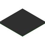
Field Programmable Gate Array (FPGA) with 350,000 logic cells and 437,200 registers, built on 28nm process technology. Features 2180 Kbit RAM, 900 multipliers (18x25), and 2 Ethernet MACs. This 676-pin FCBGA (Fine Pitch Ball Grid Array) package, measuring 27x27mm with a 1mm pin pitch, supports surface mounting and operates within a 0°C to 85°C temperature range. Includes 545 Block RAMs and 8 DLLs/PLLs, with support for LVDS, SSTL, and HSTL differential I/O standards.
PackageFCBGA
MountingSurface Mount
Quick Jump:
Technical Specifications
Xilinx XC7Z045-1FFG676C technical specifications.
General
| Basic Package Type | Ball Grid Array |
| Package Family Name | BGA |
| Package/Case | FCBGA |
| Package Description | Fine Pitch Ball Grid Array |
| Lead Shape | Ball |
| Pin Count | 676 |
| PCB | 676 |
| Package Length (mm) | 27 |
| Package Width (mm) | 27 |
| Package Height (mm) | 2.4(Max) |
| Seated Plane Height (mm) | 3(Max) |
| Pin Pitch (mm) | 1 |
| Package Material | Plastic |
| Mounting | Surface Mount |
| Jedec | MS-034AAL-1 |
| Family Name | Kintex-7 |
| Maximum Number of User I/Os | 128 |
| Number of Registers | 437200 |
| RAM Bits | 2180Kbit |
| Device Logic Cells | 350000 |
| Process Technology | 28nm |
| Ethernet MACs | 2 |
| Number of Multipliers | 900 (18x25) |
| Programmability | Yes |
| Program Memory Type | SRAM |
| Min Operating Temperature | 0°C |
| Max Operating Temperature | 85°C |
| Dedicated DSP | 900 |
| Speed Grade | 1 |
| Differential I/O Standards Supported | LVDS|SSTL|HSTL |
| Device Number of DLLs/PLLs | 8 |
| Total Number of Block RAM | 545 |
Compliance
| Cage Code | 68994 |
| EU RoHS | Yes |
| HTS Code | 8542390001 |
| Schedule B | 8542390000 |
| ECCN | 3A991.d |
| Automotive | Yes |
| RoHS Versions | 2011/65/EU, 2015/863 |
Datasheet
Xilinx XC7Z045-1FFG676C Datasheet
Download the complete datasheet for Xilinx XC7Z045-1FFG676C to view detailed technical specifications.
This datasheet cannot be embedded due to technical restrictions.
