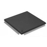
Field Programmable Gate Array (FPGA) with 4160 logic cells and 263,000 system gates. Features 52 Kbit RAM, 26 block RAMs, and 2 DLLs/PLLs. Supports LVPECL, LVDS, PCI-X, AGP, CTT, LVTTL, and LVCMOS I/O standards, with external memory interfaces for DDR SDRAM and ZBT SRAM. Housed in a 144-pin TQFP (Thin Quad Flat Package) with a 0.5mm pin pitch, suitable for surface mounting. Operates within a temperature range of 0°C to 85°C.
PackageTQFP
MountingSurface Mount
Quick Jump:
Technical Specifications
Intel EP20K100ETC144XNES technical specifications.
General
| Basic Package Type | Lead-Frame SMT |
| Package Family Name | QFP |
| Package/Case | TQFP |
| Package Description | Thin Quad Flat Package |
| Lead Shape | Gull-wing |
| Pin Count | 144 |
| PCB | 144 |
| Package Length (mm) | 20 |
| Package Width (mm) | 20 |
| Package Height (mm) | 1.4 |
| Seated Plane Height (mm) | 1.6(Max) |
| Pin Pitch (mm) | 0.5 |
| Package Material | Plastic |
| Mounting | Surface Mount |
| Jedec | MS-026BFB |
| Family Name | APEX 20K |
| Maximum Number of User I/Os | 92 |
| RAM Bits | 52Kbit |
| Device Logic Cells | 4160 |
| Process Technology | 0.22um |
| Device System Gates | 263000 |
| Programmability | No |
| Program Memory Type | SRAM |
| Min Operating Temperature | 0°C |
| Max Operating Temperature | 85°C |
| Speed Grade | STD |
| Differential I/O Standards Supported | LVPECL|LVDS|PCI-X|AGP|CTT |
| Single-Ended I/O Standards Supported | LVTTL|LVCMOS |
| External Memory Interface | DDR SDRAM|ZBT SRAM |
| Device Number of DLLs/PLLs | 2 |
| Total Number of Block RAM | 26 |
Compliance
| Cage Code | 4BA62 |
| EU RoHS | Yes |
| HTS Code | 8542390001 |
| Schedule B | 8542390000 |
| ECCN | EAR99 |
| Automotive | No |
| AEC Qualified | No |
| PPAP | No |
| Radiation Hardening | No |
| RoHS Versions | 2002/95/EC |
Datasheet
Intel EP20K100ETC144XNES Datasheet
Download the complete datasheet for Intel EP20K100ETC144XNES to view detailed technical specifications.
This datasheet cannot be embedded due to technical restrictions.