Utilizing XPT™ thin-wafer technology and 4th generation (GenX4™) Trench IGBT process, these up to 1200V devices helps to reduced gate driver requirements and conduction losses. It features reduced thermal resistance, low losses, high current densities and low gate charge requirement. A positive collector-to-emitter voltage temperature coefficient enables designers to use multiple devices in parallel.
Checking distributor stock and pricing after the page loads.
Sign in to ask questions about the Ixys IXYK110N120A4 datasheet using AI. Get instant answers about specifications, features, and technical details, ideal for finding information in larger documents.
Sign In to ChatWidest selection of semiconductors and electronic components in stock and ready to ship ™
| Collector-Emitter Voltage (V_CES) | 1200V |
| Collector Current (I_C110) @ T_C=110°C | 110A |
| Collector-Emitter Saturation Voltage Max (V_CE(sat)) | 1.80V |
| Current Fall Time Typical (t_fi(typ)) | 300ns |
| Collector-Emitter Voltage Max (V_CES) @ T_J = 25°C to 175°C | 1200V |
| Collector-Gate Voltage Max (V_CGR) @ T_J = 25°C to 175°C, R_GE = 1MΩ | 1200V |
| Gate-Emitter Voltage Max, Continuous (V_GES) | ±20V |
| Gate-Emitter Voltage Max, Transient (V_GEM) | ±30V |
| Collector Current Max (I_C25) @ T_C = 25°C (Chip Capability) | 375A |
| Terminal Current Limit (I_LRMS) | 160A |
| Pulsed Collector Current Max (I_CM) @ T_C = 25°C, 1ms | 900A |
| Reverse Bias Safe Operating Area (RBSOA) Pulsed Collector Current (I_CM) @ V_GE=15V, T_VJ=125C, R_G=2Ω | 220A |
| Reverse Bias Safe Operating Area (RBSOA) V_CE | 0.8 V_CESV |
| Total Power Dissipation Max (P_C) @ T_C = 25°C | 1360W |
| Junction Temperature Range (T_J) | -55 ... +175°C |
| Maximum Junction Temperature (T_JM) | 175°C |
| Storage Temperature Range (T_stg) | -55 ... +175°C |
| Lead Soldering Temperature (T_L) @ 1.6mm from case for 10s | 300°C |
| Mounting Torque (M_d) | 1.13/10Nm/lb.in |
| Weight | 10g |
| Collector-Emitter Breakdown Voltage (BV_CES) @ I_C=250µA, V_GE=0V | 1200V |
| Gate-Emitter Threshold Voltage (V_GE(th)) @ I_C=3mA, V_CE=V_GE | 4.5 Min 6.5 TypV |
| Collector-Emitter Cutoff Current (I_CES) @ V_CE=V_CES, V_GE=0V | 25 MaxμA |
| Collector-Emitter Cutoff Current (I_CES) @ V_CE=V_CES, V_GE=0V, T_J=125°C | 500 MaxμA |
| Gate-Emitter Leakage Current (I_GES) @ V_GE=±20V, V_CE=0V | ±200 MaxnA |
| Collector-Emitter Saturation Voltage (V_CE(sat)) @ I_C=I_C110, V_GE=15V, T_J=25°C (Note 1) | 1.45 Typ 1.80 MaxV |
| Collector-Emitter Saturation Voltage (V_CE(sat)) @ I_C=I_C110, V_GE=15V, T_J=150°C (Note 1) | 1.60 TypV |
| Transconductance (g_fs) @ I_C=60A, V_CE=10V (Note 1) | 48 Min 80 TypS |
| Input Capacitance (C_ies) @ V_CE=25V, V_GE=0V, f=1MHz | 6030 TyppF |
| Output Capacitance (C_oes) @ V_CE=25V, V_GE=0V, f=1MHz | 340 TyppF |
| Reverse Transfer Capacitance (C_res) @ V_CE=25V, V_GE=0V, f=1MHz | 225 TyppF |
| Total Gate Charge (Q_g(on)) @ I_C=I_C110, V_GE=15V, V_CE=0.5*V_CES | 305 TypnC |
| Gate-Emitter Charge (Q_ge) @ I_C=I_C110, V_GE=15V, V_CE=0.5*V_CES | 58 TypnC |
| Gate-Collector Charge (Q_gc) @ I_C=I_C110, V_GE=15V, V_CE=0.5*V_CES | 148 TypnC |
| Turn-on Delay Time (t_d(on)) @ I_C=50A, V_GE=15V, T_J=25°C (Note 2) | 42 Typns |
| Current Rise Time (t_ri) @ I_C=50A, V_GE=15V, T_J=25°C (Note 2) | 36 Typns |
| Turn-on Energy (E_on) @ I_C=50A, V_GE=15V, T_J=25°C (Note 2) | 2.5 TypmJ |
| Turn-off Delay Time (t_d(off)) @ I_C=50A, V_GE=15V, T_J=25°C (Note 2) | 550 Typns |
| Current Fall Time (t_fi) @ I_C=50A, V_GE=15V, T_J=25°C (Note 2) | 300 Typns |
| Turn-off Energy (E_off) @ I_C=50A, V_GE=15V, T_J=25°C (Note 2) | 8.4 TypmJ |
| Turn-on Delay Time (t_d(on)) @ I_C=50A, V_GE=15V, T_J=150°C (Note 2) | 35 Typns |
| Current Rise Time (t_ri) @ I_C=50A, V_GE=15V, T_J=150°C (Note 2) | 33 Typns |
| Turn-on Energy (E_on) @ I_C=50A, V_GE=15V, T_J=150°C (Note 2) | 4.4 TypmJ |
| Turn-off Delay Time (t_d(off)) @ I_C=50A, V_GE=15V, T_J=150°C (Note 2) | 700 Typns |
| Current Fall Time (t_fi) @ I_C=50A, V_GE=15V, T_J=150°C (Note 2) | 590 Typns |
| Turn-off Energy (E_off) @ I_C=50A, V_GE=15V, T_J=150°C (Note 2) | 14.0 TypmJ |
| Thermal Resistance, Junction to Case (R_thJC) | 0.11 Typ°C/W |
| Thermal Resistance, Case to Heatsink (R_thCS) | 0.15 Typ°C/W |
| Feature | Optimized for Low Conduction Losses |
| Feature | Square RBSOA |
| Feature | Positive Thermal Coefficient of Vce(sat) |
| Feature | International Standard Package |
| Advantage | High Power Density |
| Advantage | Low Gate Drive Requirement |
| Application | Power Inverters |
| Application | UPS |
| Application | Motor Drives |
| Application | SMPS |
| Application | PFC Circuits |
| Application | Battery Chargers |
| Application | Welding Machines |
| Application | Lamp Ballasts |
| Application | Inrush Current Protection Circuits |
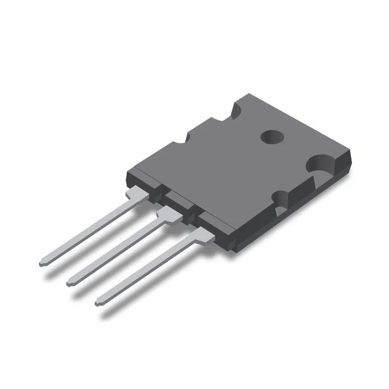
| Package Type | TO-264 (IXYK) |
| Pin Description G | Gate |
| Pin Description E | Emitter |
| Pin Description C | Collector |
| Pin Description Tab | Collector |
| Package Standard | International Standard Package |
Download the complete datasheet for Ixys IXYK110N120A4 to view detailed technical specifications.
The embedded preview will load automatically when this section scrolls into view.