N-channel enhancement mode power MOSFET featuring a 200V drain-source voltage and 18A continuous drain current. This single-element transistor is housed in a TO-220FP package with a 3-pin through-hole configuration and a tab. Key electrical characteristics include a maximum gate-source voltage of ±30V, a low drain-source on-resistance of 140mΩ at 10V, and a typical gate charge of 20nC at 10V. Maximum power dissipation is 41W, with an operating temperature range from -55°C to 150°C.
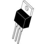
PackageTO-220FP
MountingThrough Hole
Quick Jump:
Technical Specifications
Onsemi FDPF18N20FT technical specifications.
General
| Basic Package Type | Through Hole |
| Package Family Name | TO-220 |
| Package/Case | TO-220FP |
| Package Description | Transistor Outline Package Fullpak |
| Lead Shape | Through Hole |
| Pin Count | 3 |
| PCB | 3 |
| Tab | Tab |
| Package Length (mm) | 10.16 |
| Package Width (mm) | 4.7 |
| Package Height (mm) | 15.87 |
| Seated Plane Height (mm) | 19.1 |
| Pin Pitch (mm) | 2.54 |
| Package Material | Plastic |
| Mounting | Through Hole |
| Jedec | TO-220-F |
| Configuration | Single |
| Category | Power MOSFET |
| Channel Mode | Enhancement |
| Channel Type | N |
| Number of Elements per Chip | 1 |
| Maximum Drain Source Voltage | 200V |
| Maximum Gate Source Voltage | ±30V |
| Maximum Continuous Drain Current | 18A |
| Maximum Drain Source Resistance | 140@10VmOhm |
| Typical Gate Charge @ Vgs | 20@10VnC |
| Typical Gate Charge @ 10V | 20nC |
| Typical Input Capacitance @ Vds | 885@25VpF |
| Maximum Power Dissipation | 41000mW |
| Min Operating Temperature | -55°C |
| Max Operating Temperature | 150°C |
Compliance
| Cage Code | 5V1P1 |
| EU RoHS | Yes with Exemption |
| HTS Code | 8541290095 |
| Schedule B | 8541290080 |
| ECCN | EAR99 |
| Automotive | No |
| AEC Qualified | No |
| PPAP | No |
| Radiation Hardening | No |
| RoHS Versions | 2011/65/EU, 2015/863 |
Datasheet
Onsemi FDPF18N20FT Datasheet
Download the complete datasheet for Onsemi FDPF18N20FT to view detailed technical specifications.
This datasheet cannot be embedded due to technical restrictions.