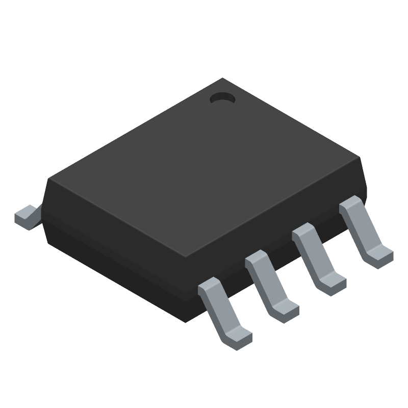
N and P-Channel MOSFET, 60V Drain to Source Breakdown Voltage, 4.5A Continuous Drain Current, 55mR Max Drain-Source On Resistance. Features 2.2V Nominal Gate to Source Voltage, 650pF Input Capacitance, and 12ns Fall Time. Packaged in SOIC for surface mount applications, this RoHS compliant component operates from -55°C to 175°C with a 2W Max Power Dissipation.
PackageSOIC
Current Rating4.5A
MountingSurface Mount
PolarityP-CHANNEL
Quick Jump:
Technical Specifications
Onsemi FDS4559 technical specifications.
General
| Package/Case | SOIC |
| Continuous Drain Current (ID) | 4.5A |
| Current Rating | 4.5A |
| Drain to Source Breakdown Voltage | 60V |
| Drain to Source Resistance | 55mR |
| Drain to Source Voltage (Vdss) | 60V |
| Drain-source On Resistance-Max | 55MR |
| Dual Supply Voltage | 60V |
| Fall Time | 12ns |
| FET Type | N and P-Channel |
| Gate to Source Voltage (Vgs) | 20V |
| Height | 1.5mm |
| Input Capacitance | 650pF |
| Lead Free | Lead Free |
| Length | 5mm |
| Max Operating Temperature | 175°C |
| Min Operating Temperature | -55°C |
| Max Power Dissipation | 2W |
| Mount | Surface Mount |
| Nominal Vgs | 2.2V |
| Number of Channels | 2 |
| Number of Elements | 2 |
| Package Quantity | 2500 |
| Packaging | Tape and Reel |
| Polarity | P-CHANNEL |
| Power Dissipation | 2W |
| Radiation Hardening | No |
| Rds On Max | 55mR |
| Reach SVHC Compliant | No |
| RoHS Compliant | Yes |
| Series | PowerTrench® |
| Termination | SMD/SMT |
| Threshold Voltage | 2.2V |
| Turn-Off Delay Time | 19ns |
| Weight | 0.187g |
| Width | 4mm |
Compliance
| RoHS | Compliant |
Datasheet
Onsemi FDS4559 Datasheet
Download the complete datasheet for Onsemi FDS4559 to view detailed technical specifications.
This datasheet cannot be embedded due to technical restrictions.
Product Images

