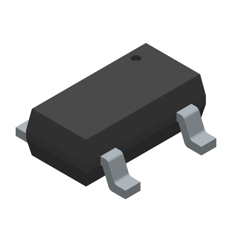
CMOS buffer IC featuring a single, non-inverting function. Operates with a supply voltage range of 2V to 5.5V, nominal 5V. Offers a propagation delay of 14.5ns (typical 10ns at nominal supply) with a load capacitance of 50pF. This 5-terminal device, housed in a 5-pin TSOP package (JEDEC R-PDSO-G5), supports a wide operating temperature range from -55°C to 125°C, suitable for military applications.
Quick Jump:
Technical Specifications
Onsemi M74VHC1GT50DTT1G technical specifications.
General
| Max Operating Temperature | 125 |
| Number of Terminals | 5 |
| Min Operating Temperature | -55 |
| Terminal Position | DUAL |
| JEDEC Package Code | R-PDSO-G5 |
| Width | 1.5 |
| Length | 3 |
| Pin Count | 5 |
| Number of Functions | 1 |
| Temperature Grade | MILITARY |
| Supply Voltage-Nom (Vsup) | 5 |
| Supply Voltage-Max (Vsup) | 5.5 |
| Supply Voltage-Min (Vsup) | 2 |
| Logic IC Type | BUFFER |
| Family | AHC/VHC |
| Propagation Delay (tpd) | 14.5 |
| Max I(ol) | 0.008 |
| Prop. Delay@Nom-Sup | 10 |
| Load Capacitance | 50 |
| Number of Inputs | 1 |
| Power Supply Current-Max (ICC) | 0.04 |
| Schmitt Trigger | NO |
Compliance
| Eccn Code | EAR99 |
| Lead Free | Yes |
| HTS Code | 8542.39.00.01 |
| REACH | Compliant |
| Military Spec | False |
Datasheet
Onsemi M74VHC1GT50DTT1G Datasheet
Download the complete datasheet for Onsemi M74VHC1GT50DTT1G to view detailed technical specifications.
This datasheet cannot be embedded due to technical restrictions.