10-output clock fanout buffer, 1:10 ratio, supporting HCSL and LVDS output logic levels. Features HCSL, LVCMOS, LVDS, LVPECL, and LVTTL input logic levels with a maximum input frequency of 400 MHz. Operates within a 3V to 3.6V supply voltage range and a temperature range of -40°C to 85°C. Packaged in a 32-pin QFN EP (Quad Flat No Lead Package, Exposed Pad) with dimensions of 5x5x0.95mm, utilizing surface mount technology.
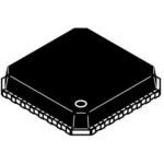
PackageQFN EP
MountingSurface Mount
Quick Jump:
Technical Specifications
Onsemi NB3N111KMNG technical specifications.
General
| Basic Package Type | Non-Lead-Frame SMT |
| Package Family Name | QFN |
| Package/Case | QFN EP |
| Package Description | Quad Flat No Lead Package, Exposed Pad |
| Lead Shape | No Lead |
| Pin Count | 32 |
| PCB | 32 |
| Package Length (mm) | 5 |
| Package Width (mm) | 5 |
| Package Height (mm) | 0.95(Max) |
| Seated Plane Height (mm) | 1(Max) |
| Pin Pitch (mm) | 0.5 |
| Package Material | Plastic |
| Mounting | Surface Mount |
| Jedec | MO-220 |
| Type | Fanout Buffer |
| Number of Outputs per Chip | 10 |
| Output Logic Level | HCSL|LVDS |
| Input Logic Level | HCSL|LVCMOS|LVDS|LVPECL|LVTTL |
| Maximum Input Frequency | 400(Typ)MHz |
| Min Operating Supply Voltage | 3V |
| Max Operating Supply Voltage | 3.6V |
| Min Operating Temperature | -40°C |
| Max Operating Temperature | 85°C |
Compliance
| Cage Code | 5V1P1 |
| EU RoHS | Yes |
| HTS Code | 8542390001 |
| Schedule B | 8542390000 |
| ECCN | EAR99 |
| Automotive | No |
| AEC Qualified | No |
| PPAP | No |
| RoHS Versions | 2011/65/EU, 2015/863 |
Datasheet
Onsemi NB3N111KMNG Datasheet
Download the complete datasheet for Onsemi NB3N111KMNG to view detailed technical specifications.
This datasheet cannot be embedded due to technical restrictions.