Precision operational amplifier featuring zero-drift architecture, ideal for automotive applications. Offers a low input offset voltage of 30 µV and a low supply current of 70 µA, enabling micropower operation. This dual-terminal, 8-terminal device boasts a 270 kHz unity gain bandwidth and a 0.15 V/µs slew rate. Operating across an automotive temperature range of -40°C to 125°C, it meets AEC-Q100 screening standards.
Checking distributor stock and pricing after the page loads.
Sign in to ask questions about the Onsemi NCV2333DMR2G datasheet using AI. Get instant answers about specifications, features, and technical details, ideal for finding information in larger documents.
Sign In to ChatWidest selection of semiconductors and electronic components in stock and ready to ship ™
Onsemi NCV2333DMR2G technical specifications.
| Max Operating Temperature | 125 |
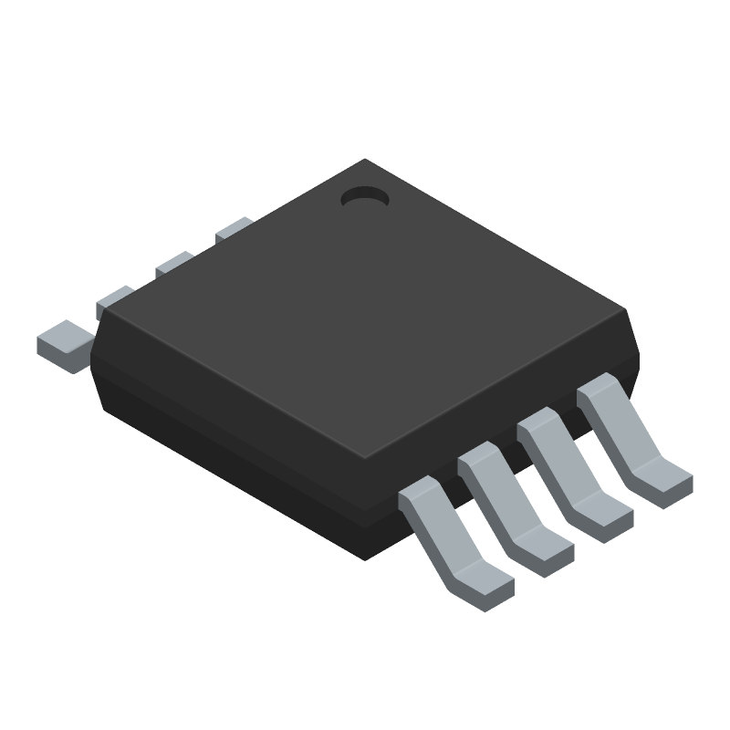
| Number of Terminals | 8 |
| Min Operating Temperature | -40 |
| Terminal Position | DUAL |
| JEDEC Package Code | S-PDSO-G8 |
| Width | 3 |
| Length | 3 |
| Number of Functions | 2 |
| Temperature Grade | AUTOMOTIVE |
| Supply Voltage-Nom (Vsup) | 3.3 |
| Supply Current-Max | 0.07 |
| Amplifier Type | OPERATIONAL AMPLIFIER |
| Supply Voltage Limit-Max | 7 |
| Input Offset Voltage-Max | 30 |
| Architecture | VOLTAGE-FEEDBACK |
| Bias Current-Max (IIB) @25C | 0.0004 |
| Slew Rate-Nom | 0.15 |
| Frequency Compensation | NO |
| Low-Offset | YES |
| Common-mode Reject Ratio-Nom | 118 |
| Voltage Gain-Min | 199526.231 |
| Unity Gain BW-Nom | 270 |
| Low-Bias | YES |
| Micropower | YES |
| Screening Level | AEC-Q100 |
| Input Offset Current-Max (IIO) | 0.0008 |
| RoHS | Yes |
| Eccn Code | EAR99 |
| Lead Free | Yes |
| HTS Code | 8542.33.00.01 |
| REACH | Compliant |
| Military Spec | False |
Download the complete datasheet for Onsemi NCV2333DMR2G to view detailed technical specifications.
The embedded preview will load automatically when this section scrolls into view.