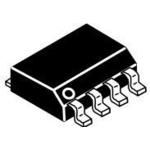
N-channel enhancement mode power MOSFET, 30V drain-source voltage, 5.5A continuous drain current. Features 24mOhm maximum drain-source resistance at 10V Vgs, 4.8nC typical gate charge at 4.5V Vgs, and 520pF typical input capacitance at 15V Vds. Housed in an 8-pin SOIC N narrow body package with gull-wing leads for surface mounting. Operates from -55°C to 150°C.
Checking distributor stock and pricing after the page loads.
Sign in to ask questions about the Onsemi NTMS4840NR2G datasheet using AI. Get instant answers about specifications, features, and technical details, ideal for finding information in larger documents.
Sign In to ChatWidest selection of semiconductors and electronic components in stock and ready to ship ™
Onsemi NTMS4840NR2G technical specifications.
| Basic Package Type | Lead-Frame SMT |
| Package Family Name | SOP |
| Package/Case | SOIC N |
| Package Description | Small Outline IC Narrow Body |
| Lead Shape | Gull-wing |
| Pin Count | 8 |
| PCB | 8 |
| Package Length (mm) | 5(Max) |
| Package Width (mm) | 4(Max) |
| Package Height (mm) | 1.5(Max) |
| Seated Plane Height (mm) | 1.75(Max) |
| Pin Pitch (mm) | 1.27 |
| Package Material | Plastic |
| Mounting | Surface Mount |
| Jedec | MS-012AA |
| Configuration | Single Quad Drain Triple Source |
| Category | Power MOSFET |
| Channel Mode | Enhancement |
| Channel Type | N |
| Number of Elements per Chip | 1 |
| Maximum Drain Source Voltage | 30V |
| Maximum Gate Source Voltage | ±20V |
| Maximum Continuous Drain Current | 5.5A |
| Maximum Drain Source Resistance | 24@10VmOhm |
| Typical Gate Charge @ Vgs | [email protected]|9.5@10VnC |
| Typical Gate Charge @ 10V | 9.5nC |
| Typical Input Capacitance @ Vds | 520@15VpF |
| Maximum Power Dissipation | 1950mW |
| Min Operating Temperature | -55°C |
| Max Operating Temperature | 150°C |
| Cage Code | 5V1P1 |
| EU RoHS | Yes |
| HTS Code | 8541290095 |
| Schedule B | 8541290080 |
| ECCN | EAR99 |
| Automotive | No |
| AEC Qualified | No |
| PPAP | No |
| Radiation Hardening | No |
| RoHS Versions | 2011/65/EU, 2015/863 |
Download the complete datasheet for Onsemi NTMS4840NR2G to view detailed technical specifications.
The embedded preview will load automatically when this section scrolls into view.