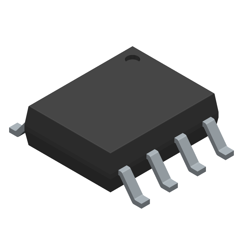
Automotive-grade, dual-channel operational amplifier featuring a 6 MHz unity-gain bandwidth and a 2.7 V/µs nominal slew rate. This voltage-feedback architecture boasts a low input offset voltage of 1400 µV maximum and a low bias current of 0.9 µA maximum, with a typical bias current of 0.3 nA at 25°C. Operating across a wide supply voltage range from 5 V nominal up to 40 V maximum, it offers a high common-mode reject ratio of 105 dB nominal and a minimum voltage gain of 177,827. The device is housed in an 8-terminal, 3.9 x 4.9 mm JEDEC R-PDSO-G8 package, suitable for operation between -40°C and 125°C.
Checking distributor stock and pricing after the page loads.
Sign in to ask questions about the Stmicroelectronics TSB712IYDT datasheet using AI. Get instant answers about specifications, features, and technical details, ideal for finding information in larger documents.
Sign In to ChatWidest selection of semiconductors and electronic components in stock and ready to ship ™
| Max Operating Temperature | 125 |
| Number of Terminals | 8 |
| Min Operating Temperature | -40 |
| Terminal Position | DUAL |
| JEDEC Package Code | R-PDSO-G8 |
| Width | 3.9 |
| Length | 4.9 |
| Number of Functions | 2 |
| Temperature Grade | AUTOMOTIVE |
| Supply Voltage-Nom (Vsup) | 5 |
| Supply Current-Max | 3 |
| Amplifier Type | OPERATIONAL AMPLIFIER |
| Supply Voltage Limit-Max | 40 |
| Input Offset Voltage-Max | 1400 |
| Average Bias Current-Max (IIB) | 0.9 |
| Architecture | VOLTAGE-FEEDBACK |
| Bias Current-Max (IIB) @25C | 0.0003 |
| Slew Rate-Nom | 2.7 |
| Frequency Compensation | YES |
| Low-Offset | YES |
| Common-mode Reject Ratio-Nom | 105 |
| Voltage Gain-Min | 177827.941 |
| Unity Gain BW-Nom | 6000 |
| Low-Bias | YES |
| Micropower | NO |
| Screening Level | AEC-Q100 |
| Slew Rate-Min | 2.2 |
| REACH | Compliant |
| Military Spec | False |
Download the complete datasheet for Stmicroelectronics TSB712IYDT to view detailed technical specifications.
The embedded preview will load automatically when this section scrolls into view.