P-channel enhancement mode MOSFET for small signal applications. Features a 20V maximum drain-source voltage and 0.1A maximum continuous drain current. This single-element transistor is housed in a 3-pin CST package with no leads, designed for surface mounting. Key specifications include a maximum gate-source voltage of ±10V, a maximum drain-source resistance of 8000 mOhm at 4V, and a typical input capacitance of 12.2 pF at 3V Vds. Operating temperature range is -55°C to 150°C.
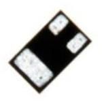
PackageCST
MountingSurface Mount
Quick Jump:
Technical Specifications
Toshiba SSM3J35CT(TPL3) technical specifications.
General
| Basic Package Type | Non-Lead-Frame SMT |
| Package/Case | CST |
| Lead Shape | No Lead |
| Pin Count | 3 |
| PCB | 3 |
| Package Length (mm) | 0.6 |
| Package Width (mm) | 1 |
| Seated Plane Height (mm) | 0.38 |
| Pin Pitch (mm) | 0.35|0.65 |
| Package Material | Plastic |
| Mounting | Surface Mount |
| Configuration | Single |
| Category | Small Signal |
| Channel Mode | Enhancement |
| Channel Type | P |
| Number of Elements per Chip | 1 |
| Maximum Drain Source Voltage | 20V |
| Maximum Gate Source Voltage | ±10V |
| Maximum Continuous Drain Current | 0.1A |
| Material | Si |
| Maximum Gate Threshold Voltage | 1V |
| Maximum Drain Source Resistance | 8000@4VmOhm |
| Typical Input Capacitance @ Vds | 12.2@3VpF |
| Maximum Power Dissipation | 100mW |
| Min Operating Temperature | -55°C |
| Max Operating Temperature | 150°C |
Compliance
| Cage Code | S0562 |
| EU RoHS | Yes |
| HTS Code | 8541210095 |
| Schedule B | 8541210080 |
| ECCN | EAR99 |
| Automotive | No |
| AEC Qualified | No |
| PPAP | No |
| RoHS Versions | 2011/65/EU, 2015/863 |
Datasheet
Toshiba SSM3J35CT(TPL3) Datasheet
Download the complete datasheet for Toshiba SSM3J35CT(TPL3) to view detailed technical specifications.
This datasheet cannot be embedded due to technical restrictions.