P-channel Power MOSFET featuring TrenchFET technology, designed for surface mount applications. This dual dual-source device operates with a maximum drain-source voltage of 30V and a continuous drain current of 2.5A. Housed in an 8-pin TSSOP package with gull-wing leads, it offers a low seated plane height of 1.2mm (Max) and a 0.65mm pin pitch. Key electrical characteristics include a maximum drain-source on-resistance of 80mOhm at 10V and a typical gate charge of 5.8nC at 10V. Operating temperature range spans from -55°C to 150°C.
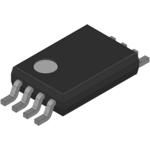
PackageTSSOP
MountingSurface Mount
Quick Jump:
Technical Specifications
Vishay SI6955ADQ-T1-GE3 technical specifications.
General
| Basic Package Type | Lead-Frame SMT |
| Package Family Name | SOP |
| Package/Case | TSSOP |
| Package Description | Thin Shrink Small Outline Package |
| Lead Shape | Gull-wing |
| Pin Count | 8 |
| PCB | 8 |
| Package Length (mm) | 3 |
| Package Width (mm) | 4.4 |
| Package Height (mm) | 1 |
| Seated Plane Height (mm) | 1.2(Max) |
| Pin Pitch (mm) | 0.65 |
| Package Material | Plastic |
| Mounting | Surface Mount |
| Jedec | MO-153AA |
| Configuration | Dual Dual Source |
| Category | Power MOSFET |
| Channel Mode | Enhancement |
| Channel Type | P |
| Number of Elements per Chip | 2 |
| Process Technology | TrenchFET |
| Maximum Drain Source Voltage | 30V |
| Maximum Gate Source Voltage | ±20V |
| Maximum Continuous Drain Current | 2.5A |
| Maximum Gate Threshold Voltage | 1(Min)V |
| Maximum Drain Source Resistance | 80@10VmOhm |
| Typical Gate Charge @ Vgs | 5.8@10VnC |
| Typical Gate Charge @ 10V | 5.8nC |
| Maximum Power Dissipation | 1140mW |
| Min Operating Temperature | -55°C |
| Max Operating Temperature | 150°C |
Compliance
| Cage Code | 18612 |
| EU RoHS | Yes |
| HTS Code | 8541210095 |
| Schedule B | 8541210080 |
| ECCN | EAR99 |
| Automotive | No |
| AEC Qualified | No |
| PPAP | No |
| Radiation Hardening | No |
| RoHS Versions | 2011/65/EU, 2015/863 |
Datasheet
Vishay SI6955ADQ-T1-GE3 Datasheet
Download the complete datasheet for Vishay SI6955ADQ-T1-GE3 to view detailed technical specifications.
This datasheet cannot be embedded due to technical restrictions.