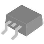
N-channel enhancement mode power MOSFET featuring a 25V drain-source voltage and 66A continuous drain current. This single-element transistor is housed in a TO-252 DPAK package with a 3-pin gull-wing lead configuration for surface mounting. Key electrical characteristics include a low 9mOhm maximum drain-source resistance at 10V and a typical gate charge of 23nC at 5V. The plastic DPAK package measures 6.5mm x 5.7mm x 2.3mm, supporting a maximum power dissipation of 66W across an operating temperature range of -55°C to 150°C.
PackageDPAK
MountingSurface Mount
Quick Jump:
Technical Specifications
Advanced Power Electronics AP70L02H technical specifications.
General
| Basic Package Type | Lead-Frame SMT |
| Package Family Name | TO-252 |
| Package/Case | DPAK |
| Package Description | Deca Watt Package |
| Lead Shape | Gull-wing |
| Pin Count | 3 |
| PCB | 2 |
| Tab | Tab |
| Package Length (mm) | 6.5 |
| Package Width (mm) | 5.7 |
| Package Height (mm) | 2.3 |
| Seated Plane Height (mm) | 2.4 |
| Pin Pitch (mm) | 2.3 |
| Package Material | Plastic |
| Mounting | Surface Mount |
| Jedec | TO-252AA |
| Configuration | Single |
| Category | Power MOSFET |
| Channel Mode | Enhancement |
| Channel Type | N |
| Number of Elements per Chip | 1 |
| Maximum Drain Source Voltage | 25V |
| Maximum Gate Source Voltage | ±20V |
| Maximum Continuous Drain Current | 66A |
| Maximum Drain Source Resistance | 9@10VmOhm |
| Typical Gate Charge @ Vgs | 23@5VnC |
| Typical Input Capacitance @ Vds | 790@25VpF |
| Maximum Power Dissipation | 66000mW |
| Min Operating Temperature | -55°C |
| Max Operating Temperature | 150°C |
Compliance
| EU RoHS | Yes |
| HTS Code | 8541290095 |
| Schedule B | 8541290080 |
| ECCN | EAR99 |
| Radiation Hardening | No |
| RoHS Versions | 2011/65/EU, 2015/863 |
Datasheet
Advanced Power Electronics AP70L02H Datasheet
Download the complete datasheet for Advanced Power Electronics AP70L02H to view detailed technical specifications.
This datasheet cannot be embedded due to technical restrictions.