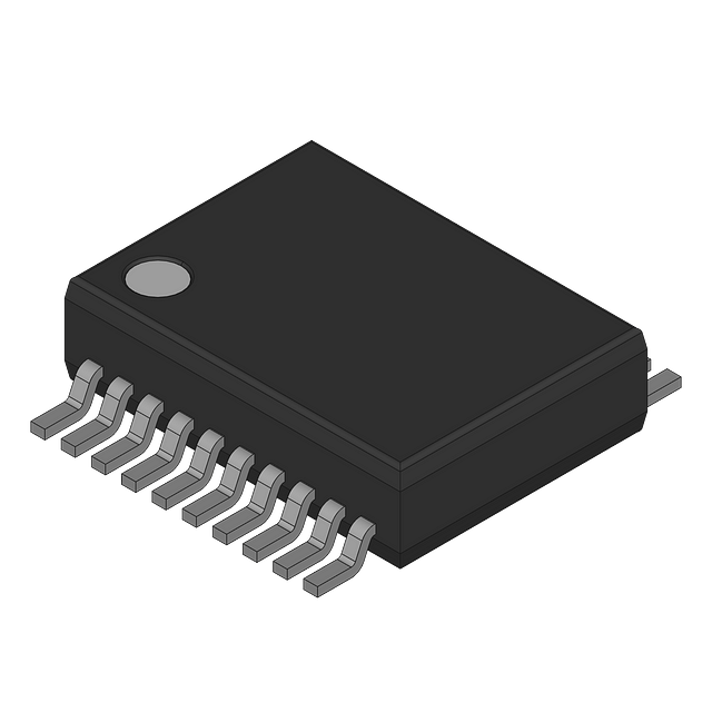
High-performance clock driver featuring 10 true CMOS outputs and a maximum frequency of 650MHz. This integrated circuit operates with a supply voltage range of 2.5V to 3.3V, offering a propagation delay of 3.5ns and a turn-on delay time of 3.5ns. Packaged in a lead-free SSOP-20 with dimensions of 7.4mm (L) x 5.6mm (W) x 1.85mm (H), it supports tin, gold, and matte contact plating. The device boasts a maximum power dissipation of 750mW and operates within a temperature range of -40°C to 85°C, with a quiescent current of 25mA.
Checking distributor stock and pricing after the page loads.
Sign in to ask questions about the Cypress CY2CC810OXI datasheet using AI. Get instant answers about specifications, features, and technical details, ideal for finding information in larger documents.
Sign In to ChatWidest selection of semiconductors and electronic components in stock and ready to ship ™
Cypress CY2CC810OXI technical specifications.
| Package/Case | SSOP |
| Contact Plating | Tin, Gold, Matte |
| Height | 1.85mm |
| Input | LVCMOS |
| Lead Free | Lead Free |
| Length | 7.4mm |
| Max Frequency | 650MHz |
| Max Operating Temperature | 85°C |
| Min Operating Temperature | -40°C |
| Max Power Dissipation | 750mW |
| Max Supply Voltage | 3.3V |
| Min Supply Voltage | 2.5V |
| Number of Circuits | 1 |
| Number of Outputs | 10 |
| Operating Supply Voltage | 2.5V |
| Package Quantity | 66 |
| Packaging | Rail/Tube |
| Power Dissipation | 750mW |
| Propagation Delay | 3.5ns |
| Quiescent Current | 25mA |
| Radiation Hardening | No |
| RoHS Compliant | Yes |
| Series | CY2CC810OXI |
| Supply Voltage-Nom | 3.3V |
| Turn-On Delay Time | 3.5ns |
| Width | 5.6mm |
| RoHS | Compliant |
Download the complete datasheet for Cypress CY2CC810OXI to view detailed technical specifications.
The embedded preview will load automatically when this section scrolls into view.