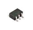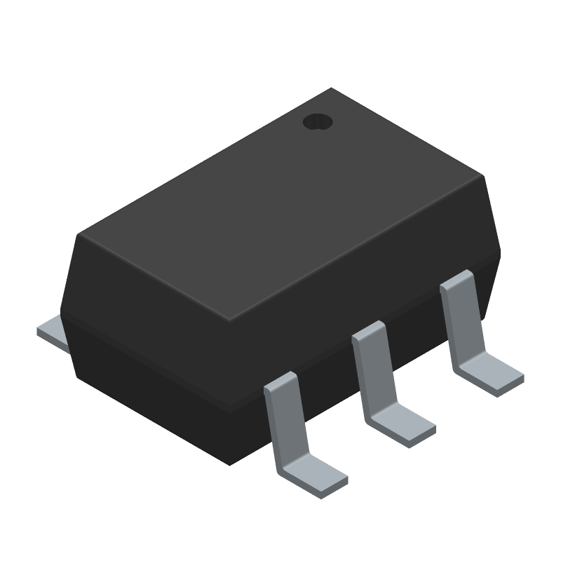
Surface mount dual N-channel and P-channel silicon JFET with 60V dual supply voltage and 115mA continuous drain current. Features a 2.5V threshold voltage, 10 Ohm maximum drain-source on-resistance, and 50pF input capacitance. Operates within a -55°C to 150°C temperature range, with 200mW maximum power dissipation. Packaged in a 6-pin SOT-363 plastic package with tin, matte contact plating.
Checking distributor stock and pricing after the page loads.
Sign in to ask questions about the Diodes BSS8402DW-7-F datasheet using AI. Get instant answers about specifications, features, and technical details, ideal for finding information in larger documents.
Sign In to ChatWidest selection of semiconductors and electronic components in stock and ready to ship ™
| Package/Case | SOT-363 |
| Contact Plating | Tin, Matte |
| Continuous Drain Current (ID) | 115mA |
| Current Rating | 115mA |
| Drain to Source Resistance | 4.4R |
| Drain to Source Voltage (Vdss) | -50V |
| Drain-source On Resistance-Max | 10R |
| Dual Supply Voltage | 60V |
| FET Type | N and P-Channel |
| Gate to Source Voltage (Vgs) | 20V |
| Height | 1mm |
| Input Capacitance | 50pF |
| Lead Free | Lead Free |
| Length | 2.2mm |
| Max Operating Temperature | 150°C |
| Min Operating Temperature | -55°C |
| Max Power Dissipation | 200mW |
| Mount | Surface Mount |
| Nominal Vgs | 2.5V |
| Number of Channels | 2 |
| Number of Elements | 2 |
| Package Quantity | 3000 |
| Packaging | Tape and Reel |
| Polarity | N-CHANNEL, P-CHANNEL |
| Power Dissipation | 200mW |
| Rds On Max | 7.5R |
| Reach SVHC Compliant | No |
| RoHS Compliant | Yes |
| Termination | SMD/SMT |
| Threshold Voltage | 2.5V |
| Turn-Off Delay Time | 18ns |
| Turn-On Delay Time | 10ns |
| Weight | 0.000212oz |
| Width | 1.35mm |
| RoHS | Compliant |
Download the complete datasheet for Diodes BSS8402DW-7-F to view detailed technical specifications.
The embedded preview will load automatically when this section scrolls into view.