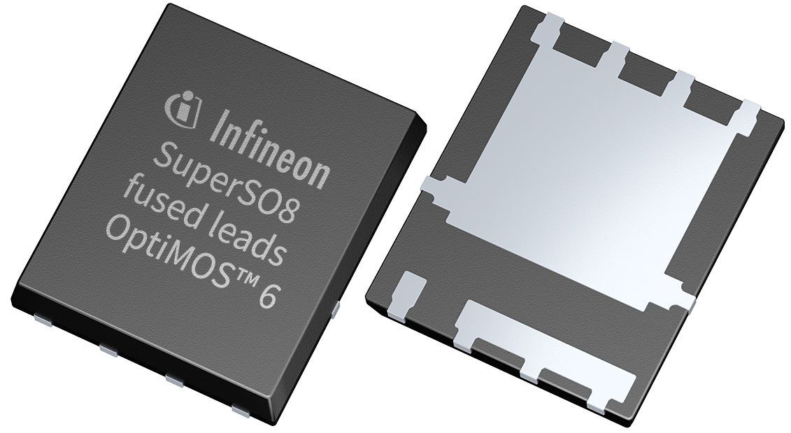
This device is an 80 V N-channel power MOSFET built on OptiMOS™ 6 technology and supplied in a SuperSO8 FL package. It is specified for up to 145 A continuous drain current at 25 °C case temperature and provides a maximum drain-source on-resistance of 3.1 mΩ at 10 V gate drive, with 2.6 mΩ typical. Typical total gate charge is 37 nC and typical reverse recovery charge is 34 nC, supporting high-frequency switching and synchronous rectification applications. The operating junction and storage temperature range is -55 °C to 175 °C, and the device is listed as RoHS compliant and halogen-free.
Checking distributor stock and pricing after the page loads.
| Drain-Source Voltage | 80V |
| Continuous Drain Current | 145A |
| Drain-Source On-Resistance (max @10V) | 3.1mΩ |
| Drain-Source On-Resistance (typ @10V) | 2.6mΩ |
| Total Gate Charge | 37nC |
| Output Charge | 73nC |
| Gate Threshold Voltage (min) | 2.4V |
| Gate Threshold Voltage (typ) | 3.0V |
| Gate Threshold Voltage (max) | 3.5V |
| Operating Temperature Min | -55°C |
| Operating Temperature Max | 175°C |
| Input Capacitance | 2600pF |
| Output Capacitance | 880pF |
| Reverse Transfer Capacitance | 24pF |
| Reverse Recovery Charge | 34nC |
| Reverse Recovery Time | 36ns |
| Thermal Resistance Junction-Case | 0.5°C/W |
| Avalanche Energy | 387mJ |
| RoHS | Compliant |
| Halogen Free | Yes |
| Lead-free | No |
These are design resources that include the Infineon ISC031N08NM6
750W isolated quarter-brick DC-DC converter reference design for 5G RFPA applications, converting 48V to 50V with 95.3% efficiency using the XDPP1100 digital controller.
