This industrial-grade clock driver IC features a 20-pin TSSOP package and operates within a temperature range of -40°C to 85°C. It has a nominal supply voltage of 3.3V, with a maximum and minimum supply voltage of 3.465V and 3.135V, respectively. The IC has a propagation delay of 0.15 units, with a propagation delay at nominal supply voltage also measured at 0.15 units. It is a PLL-based clock driver with a single function and is part of the 9DB family.
Checking distributor stock and pricing after the page loads.
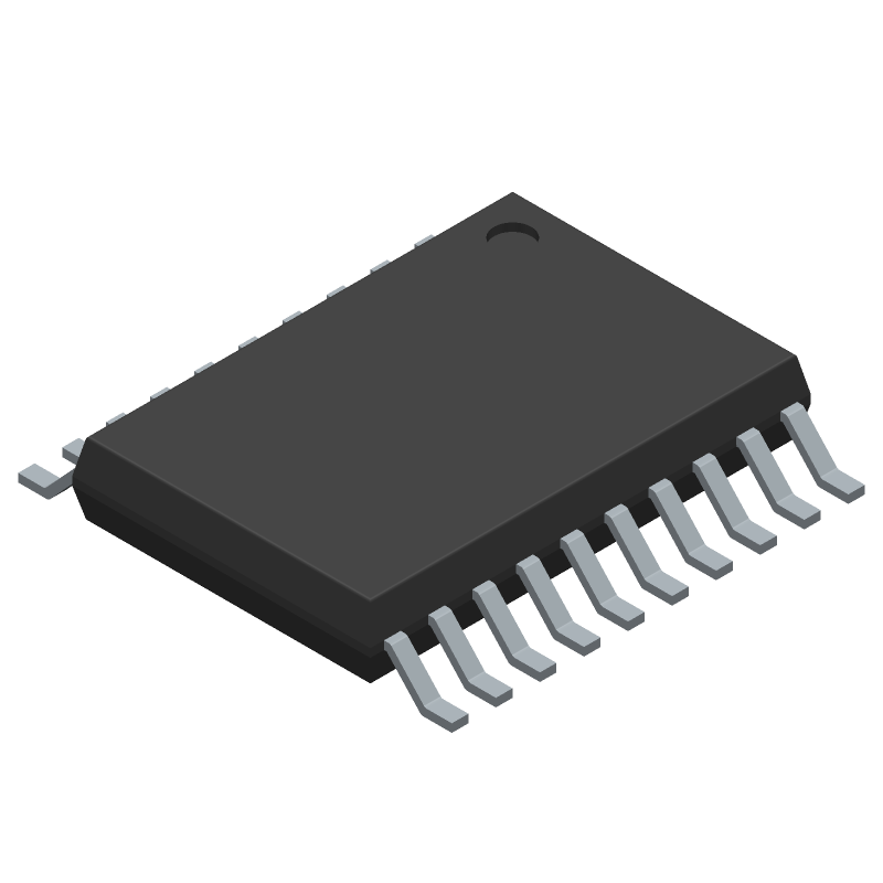
Integrated Device Technology 9DB102BGILFT technical specifications.
| Max Operating Temperature | 85 |
| Number of Terminals | 20 |
| Min Operating Temperature | -40 |
| Terminal Position | DUAL |
| JEDEC Package Code | R-PDSO-G20 |
| Width | 4.4 |
| Length | 6.5 |
| Pin Count | 20 |
| Number of Functions | 1 |
| Temperature Grade | INDUSTRIAL |
| Supply Voltage-Nom (Vsup) | 3.3 |
| Supply Voltage-Max (Vsup) | 3.465 |
| Supply Voltage-Min (Vsup) | 3.135 |
| Logic IC Type | PLL BASED CLOCK DRIVER |
| Family | 9DB |
| Propagation Delay (tpd) | 0.15 |
| Prop. Delay@Nom-Sup | 0.15 |
| RoHS | Yes |
| Eccn Code | EAR99 |
| Lead Free | Yes |
| HTS Code | 8542.39.00.01 |
| REACH | Compliant |
| Military Spec | False |