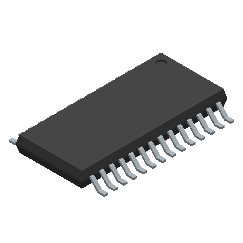
The 9DB106BGLF is a commercial-grade PLL-based clock driver IC with a maximum operating temperature of 70 degrees Celsius and a minimum operating temperature of 0 degrees Celsius. It has 28 terminals and a supply voltage range of 3.135 to 3.465 volts. The IC is packaged in a 28-pin TSSOP package with a width of 4.4 millimeters and a length of 9.7 millimeters. It has a propagation delay of 0.15 nanoseconds and is suitable for use in commercial applications.
Integrated Device Technology 9DB106BGLF technical specifications.
| Max Operating Temperature | 70 |
| Number of Terminals | 28 |
| Min Operating Temperature | 0 |
| Terminal Position | DUAL |
| JEDEC Package Code | R-PDSO-G28 |
| Width | 4.4 |
| Length | 9.7 |
| Pin Count | 28 |
| Number of Functions | 1 |
| Temperature Grade | COMMERCIAL |
| Supply Voltage-Nom (Vsup) | 3.3 |
| Supply Voltage-Max (Vsup) | 3.465 |
| Supply Voltage-Min (Vsup) | 3.135 |
| Logic IC Type | PLL BASED CLOCK DRIVER |
| Family | 9DB |
| Propagation Delay (tpd) | 0.15 |
| Prop. Delay@Nom-Sup | 0.15 |
| RoHS | Yes |
| Eccn Code | EAR99 |
| Lead Free | Yes |
| HTS Code | 8542.39.00.01 |
| REACH | Compliant |
| Military Spec | False |
No datasheet is available for this part.