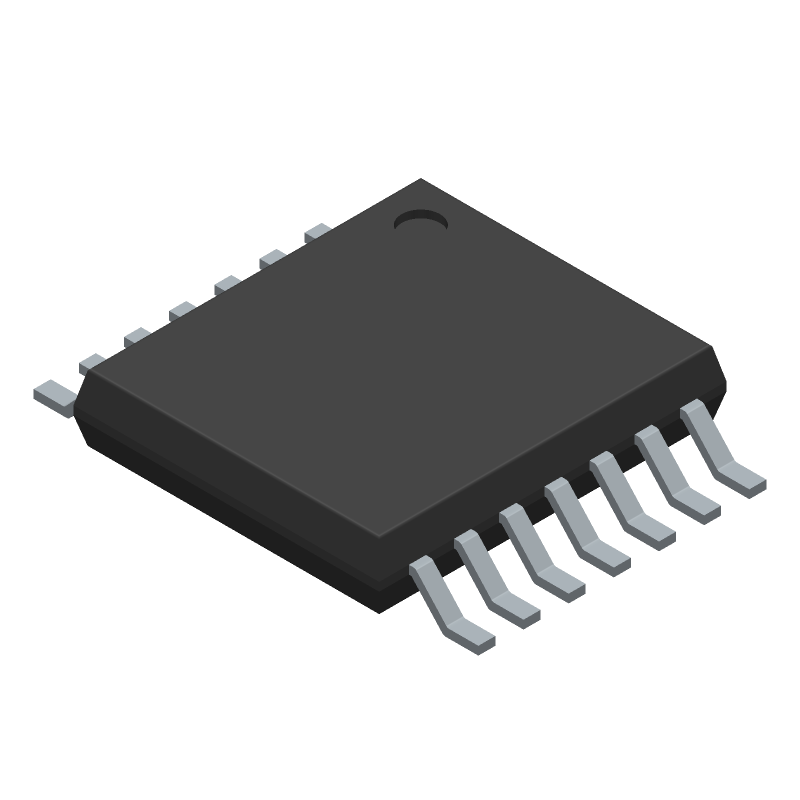
The 74LVC00APW,112 is a dual NAND gate logic IC from Nexperia, featuring 14 terminals and a TSSOP package. It operates within a temperature range of -40 to 125°C and is compliant with AEC-Q100. The device has a supply voltage range of 1.2 to 3.6V and a propagation delay of 6.5ns. It is designed for use in automotive applications and is part of the LVC/LCX/Z family.
Sign in to ask questions about the Nexperia 74LVC00APW,112 datasheet using AI. Get instant answers about specifications, features, and technical details, ideal for finding information in larger documents.
Sign In to ChatWidest selection of semiconductors and electronic components in stock and ready to ship ™
Nexperia 74LVC00APW,112 technical specifications.
| Max Operating Temperature | 125 |
| Number of Terminals | 14 |
| Min Operating Temperature | -40 |
| Terminal Position | DUAL |
| JEDEC Package Code | R-PDSO-G14 |
| Width | 4.4 |
| Length | 5 |
| Pin Count | 14 |
| Number of Functions | 4 |
| Temperature Grade | AUTOMOTIVE |
| Supply Voltage-Nom (Vsup) | 2.7 |
| Supply Voltage-Max (Vsup) | 3.6 |
| Supply Voltage-Min (Vsup) | 1.2 |
| Logic IC Type | NAND GATE |
| Family | LVC/LCX/Z |
| Propagation Delay (tpd) | 6.5 |
| Number of Inputs | 2 |
| HTS Code | 8542.39.00.01 |
| REACH | Compliant |
| Military Spec | False |
Download the complete datasheet for Nexperia 74LVC00APW,112 to view detailed technical specifications.
The embedded preview will load automatically when this section scrolls into view.