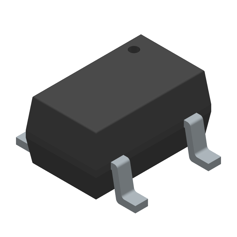
The 74LVC1G08GW,125 is an AND gate logic IC from Nexperia. It operates over a temperature range of -40°C to 125°C and is available in a 5-pin SOP package. The device has a propagation delay of 10.5ns and can handle supply voltages from 1.65V to 5.5V. It is designed for automotive applications and is compliant with various industry standards.
Quick Jump:
Chat with Datasheet
Sponsored by
Sign in to ask questions about the Nexperia 74LVC1G08GW,125 datasheet using AI. Get instant answers about specifications, features, and technical details, ideal for finding information in larger documents.
Sign In to ChatWidest selection of semiconductors and electronic components in stock and ready to ship ™
Technical Specifications
Nexperia 74LVC1G08GW,125 technical specifications.
General
| Max Operating Temperature | 125 |
| Number of Terminals | 5 |
| Min Operating Temperature | -40 |
| Terminal Position | DUAL |
| JEDEC Package Code | R-PDSO-G5 |
| Width | 1.25 |
| Length | 2.05 |
| Pin Count | 5 |
| Number of Functions | 1 |
| Temperature Grade | AUTOMOTIVE |
| Supply Voltage-Nom (Vsup) | 1.8 |
| Supply Voltage-Max (Vsup) | 5.5 |
| Supply Voltage-Min (Vsup) | 1.65 |
| Logic IC Type | AND GATE |
| Family | LVC/LCX/Z |
| Propagation Delay (tpd) | 10.5 |
| Number of Inputs | 2 |
Compliance
| RoHS | Yes |
| Eccn Code | EAR99 |
| HTS Code | 8542.39.00.01 |
| REACH | Compliant |
| Military Spec | False |
Datasheet
Nexperia 74LVC1G08GW,125 Datasheet
Download the complete datasheet for Nexperia 74LVC1G08GW,125 to view detailed technical specifications.
The embedded preview will load automatically when this section scrolls into view.