Dual positive-edge-triggered D-type flip-flop provides individual data, clock, set, and reset inputs with complementary outputs. The CMOS logic device operates from a 2.0 V to 6.0 V supply and supports a typical 82 MHz maximum frequency with 14 ns propagation delay. Inputs include clamp diodes for interfacing through current-limiting resistors, and the clock input uses Schmitt-trigger action for tolerance of slower rise and fall times. Operation is specified from -40 °C to +125 °C, with JEDEC compliance, latch-up performance above 100 mA, and ESD protection above 2000 V HBM and 1000 V CDM.
Checking distributor stock and pricing after the page loads.
Sign in to ask questions about the NXP 74HC74 datasheet using AI. Get instant answers about specifications, features, and technical details, ideal for finding information in larger documents.
Sign In to ChatWidest selection of semiconductors and electronic components in stock and ready to ship ™
| Function | Dual positive-edge-triggered D-type flip-flop with set and reset |
| Supply Voltage | 2.0 to 6.0V |
| Logic Switching Levels | CMOS |
| Output Drive Capability | ±5.2mA |
| Propagation Delay | 14ns |
| Maximum Frequency | 82MHz |
| Power Dissipation Consideration | Low |
| Operating Ambient Temperature | -40 to +125°C |
| Latch-up Performance | >100 per JESD 78 Class II Level BmA |
| ESD Protection HBM | >2000, ANSI/ESDA/JEDEC JS-001 class 2V |
| ESD Protection CDM | >1000, ANSI/ESDA/JEDEC JS-002 class C3V |
| JEDEC Standards | JESD8C, JESD7A |
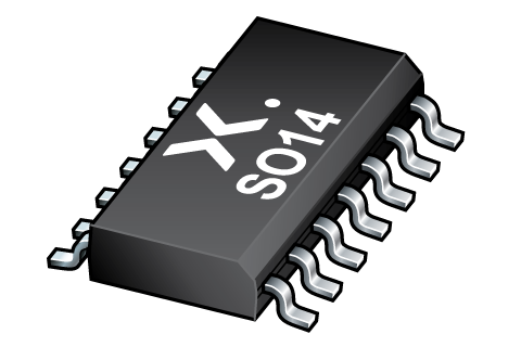
| Available Active Packages | DHVQFN14, SO14, TSSOP14 |
Download the complete datasheet for NXP 74HC74 to view detailed technical specifications.
The embedded preview will load automatically when this section scrolls into view.
These are design resources that include the NXP 74HC74
Application note for the NXP SA639 FM/IF system, featuring evaluation board design, circuit diagrams, and performance testing for DECT and high-speed GFSK applications.