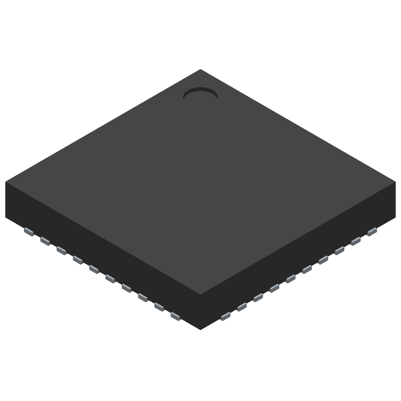
NFC/RFID read/write IC operating at 13.56MHz. Features a 40-pin HVQFN EP package with a supply voltage range of 1.65V to 1.95V. Designed for operation across a temperature range of -30°C to 85°C. The component utilizes a QUAD terminal position and is housed in a 6mm x 6mm JEDEC S-PQCC-N40 package.
Checking distributor stock and pricing after the page loads.
Sign in to ask questions about the NXP PN7150B0HN/C11002Y datasheet using AI. Get instant answers about specifications, features, and technical details, ideal for finding information in larger documents.
Sign In to ChatWidest selection of semiconductors and electronic components in stock and ready to ship ™
NXP PN7150B0HN/C11002Y technical specifications.
| Max Operating Temperature | 85 |
| Number of Terminals | 40 |
| Min Operating Temperature | -30 |
| Terminal Position | QUAD |
| JEDEC Package Code | S-PQCC-N40 |
| Width | 6 |
| Length | 6 |
| Pin Count | 40 |
| Number of Functions | 1 |
| Temperature Grade | OTHER |
| Supply Voltage-Max (Vsup) | 1.95 |
| Supply Voltage-Min (Vsup) | 1.65 |
| RoHS | Yes |
| REACH | Compliant |
| Military Spec | False |
Download the complete datasheet for NXP PN7150B0HN/C11002Y to view detailed technical specifications.
The embedded preview will load automatically when this section scrolls into view.