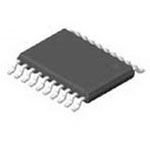
2-output HCSL differential clock driver, featuring a 20-pin TSSOP surface-mount package with gull-wing leads. This integrated circuit offers a zero-delay buffer function, supporting input frequencies from 99 MHz to 101 MHz with a maximum cycle-to-cycle jitter of 35 ps and maximum output skew of 25 ps. It operates within a temperature range of -40 °C to 85 °C and includes spread spectrum capability. The thin shrink small outline package measures 6.5mm x 4.4mm x 1mm with a 0.65mm pin pitch.
Sign in to ask questions about the Renesas 9DB102BGILF datasheet using AI. Get instant answers about specifications, features, and technical details, ideal for finding information in larger documents.
Sign In to ChatWidest selection of semiconductors and electronic components in stock and ready to ship ™
Renesas 9DB102BGILF technical specifications.
| Basic Package Type | Lead-Frame SMT |
| Package Family Name | SOP |
| Package/Case | TSSOP |
| Package Description | Thin Shrink Small Outline Package |
| Lead Shape | Gull-wing |
| Pin Count | 20 |
| PCB | 20 |
| Package Length (mm) | 6.5 |
| Package Width (mm) | 4.4 |
| Package Height (mm) | 1 |
| Seated Plane Height (mm) | 1.1 |
| Pin Pitch (mm) | 0.65 |
| Package Material | Plastic |
| Mounting | Surface Mount |
| Jedec | MO-153AC |
| Type | Clock Driver |
| Number of Inputs | 1 |
| Number of Outputs | 2 |
| Input Signal Type | Differential |
| Output Signal Type | Differential |
| Output Logic Level | HCSL |
| Minimum Input Frequency | 99MHz |
| Maximum Input Frequency | 101MHz |
| Minimum Output Frequency | 99MHz |
| Maximum Output Frequency | 101MHz |
| Maximum Cycle to Cycle Jitter | 35ps |
| Maximum Duty Cycle | 55% |
| Maximum Fall Time | 0.7ns |
| Maximum Rise Time | 0.7ns |
| Maximum Output Skew | 25ps |
| Spread Spectrum | Yes |
| Min Operating Temperature | -40°C |
| Max Operating Temperature | 85°C |
| Cage Code | SAN34 |
| EU RoHS | Yes |
| HTS Code | 8542390001 |
| Schedule B | 8542390000 |
| ECCN | EAR99 |
| Automotive | No |
| AEC Qualified | No |
| PPAP | No |
| Radiation Hardening | No |
| RoHS Versions | 2011/65/EU, 2015/863 |
Download the complete datasheet for Renesas 9DB102BGILF to view detailed technical specifications.
The embedded preview will load automatically when this section scrolls into view.