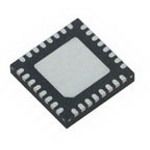
Clock driver featuring a zero-delay buffer with 4 differential LP-HCSL outputs. This surface-mount component is housed in a 32-pin VFQFPN EP package (5x5x0.88mm) with a 0.5mm pin pitch. It accepts a single differential HCSL input signal and operates across a frequency range of 30 MHz to 137.5 MHz. Key performance specifications include a maximum cycle-to-cycle jitter of 25 ps and maximum output skew of 50 ps. Operating temperature range is -40°C to 85°C.
Checking distributor stock and pricing after the page loads.
Sign in to ask questions about the Renesas 9DBV0431AKILF datasheet using AI. Get instant answers about specifications, features, and technical details, ideal for finding information in larger documents.
Sign In to ChatWidest selection of semiconductors and electronic components in stock and ready to ship ™
Renesas 9DBV0431AKILF technical specifications.
| Basic Package Type | Non-Lead-Frame SMT |
| Package Family Name | QFN |
| Package/Case | VFQFPN EP |
| Package Description | Very Fine Quad Flat Package No Lead, Exposed Pad |
| Lead Shape | No Lead |
| Pin Count | 32 |
| PCB | 32 |
| Package Length (mm) | 5 |
| Package Width (mm) | 5 |
| Package Height (mm) | 0.88 |
| Seated Plane Height (mm) | 0.9 |
| Pin Pitch (mm) | 0.5 |
| Package Material | Plastic |
| Mounting | Surface Mount |
| Type | Clock Driver |
| Number of Inputs | 1 |
| Number of Outputs | 4 |
| Input Signal Type | Differential |
| Output Signal Type | Differential |
| Input Logic Level | HCSL |
| Output Logic Level | LP-HCSL |
| Minimum Input Frequency | 30MHz |
| Maximum Input Frequency | 137.5MHz |
| Minimum Output Frequency | 30MHz |
| Maximum Output Frequency | 137.5MHz |
| Maximum Cycle to Cycle Jitter | 25ps |
| Maximum Duty Cycle | 55% |
| Maximum Output Skew | 50ps |
| Spread Spectrum | No |
| Min Operating Temperature | -40°C |
| Max Operating Temperature | 85°C |
| Cage Code | SAN34 |
| EU RoHS | Yes |
| HTS Code | 8542390001 |
| Schedule B | 8542390000 |
| ECCN | EAR99 |
| Automotive | No |
| AEC Qualified | No |
| PPAP | No |
| RoHS Versions | 2011/65/EU, 2015/863 |
Download the complete datasheet for Renesas 9DBV0431AKILF to view detailed technical specifications.
The embedded preview will load automatically when this section scrolls into view.