Dual supply, ultra-low noise, low distortion operational amplifier with rail-to-rail output. Features a voltage-feedback architecture and a 10-pin S-PDSO-G10 package. Offers a wide operating temperature range of -40°C to 125°C, nominal supply voltage of 5V, and a maximum supply voltage of 5.5V. Key specifications include a maximum input offset voltage of 840µV, nominal slew rate of 17V/µs, and a minimum voltage gain of 79432.82. Designed for automotive applications.
Sign in to ask questions about the Renesas ISL28291FUZ-T7 datasheet using AI. Get instant answers about specifications, features, and technical details, ideal for finding information in larger documents.
Sign In to ChatWidest selection of semiconductors and electronic components in stock and ready to ship ™
Renesas ISL28291FUZ-T7 technical specifications.
| Max Operating Temperature | 125 |
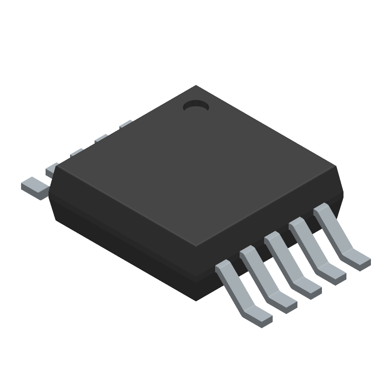
| Number of Terminals | 10 |
| Min Operating Temperature | -40 |
| Terminal Position | DUAL |
| JEDEC Package Code | S-PDSO-G10 |
| Width | 3 |
| Length | 3 |
| Pin Count | 10 |
| Number of Functions | 2 |
| Temperature Grade | AUTOMOTIVE |
| Supply Voltage-Nom (Vsup) | 5 |
| Supply Current-Max | 7 |
| Amplifier Type | OPERATIONAL AMPLIFIER |
| Supply Voltage Limit-Max | 5.5 |
| Input Offset Voltage-Max | 840 |
| Average Bias Current-Max (IIB) | 7 |
| Architecture | VOLTAGE-FEEDBACK |
| Bias Current-Max (IIB) @25C | 6 |
| Slew Rate-Nom | 17 |
| Frequency Compensation | NO |
| Low-Offset | YES |
| Common-mode Reject Ratio-Nom | 65 |
| Voltage Gain-Min | 79432.82 |
| Low-Bias | NO |
| Micropower | NO |
| Slew Rate-Min | 12 |
| Input Offset Current-Max (IIO) | 0.9 |
| Eccn Code | EAR99 |
| HTS Code | 8542.33.00.01 |
| REACH | Compliant |
| Military Spec | False |
Download the complete datasheet for Renesas ISL28291FUZ-T7 to view detailed technical specifications.
The embedded preview will load automatically when this section scrolls into view.