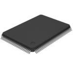
Synchronous SRAM chip with 8M-bit density, organized as 512K words by 18 bits. Features a 6.5 ns maximum access time and operates at a maximum clock rate of 133.33 MHz with SDR data rate architecture. This dual-port memory component utilizes a 19-bit address bus and is housed in a 100-pin TQFP (Thin Quad Flat Package) with a 0.65 mm pin pitch, suitable for surface mounting. It operates from a 3.3 V supply voltage, with a minimum of 3.135 V and a maximum of 3.465 V, and functions within a temperature range of 0 °C to 70 °C.
Checking distributor stock and pricing after the page loads.
Sign in to ask questions about the Samsung K7M801825B-QC265 datasheet using AI. Get instant answers about specifications, features, and technical details, ideal for finding information in larger documents.
Sign In to ChatWidest selection of semiconductors and electronic components in stock and ready to ship ™
| Basic Package Type | Lead-Frame SMT |
| Package Family Name | QFP |
| Package/Case | TQFP |
| Package Description | Thin Quad Flat Package |
| Lead Shape | Gull-wing |
| Pin Count | 100 |
| PCB | 100 |
| Package Length (mm) | 20 |
| Package Width (mm) | 14 |
| Package Height (mm) | 1.4 |
| Seated Plane Height (mm) | 1.6(Max) |
| Pin Pitch (mm) | 0.65 |
| Package Material | Plastic |
| Mounting | Surface Mount |
| Jedec | MS-026BHA |
| Density | 8Mbit |
| Address Bus Width | 19bit |
| Maximum Access Time | 6.5ns |
| Timing Type | Synchronous |
| Maximum Clock Rate | 133.33MHz |
| Data Rate Architecture | SDR |
| Density in Bits | 8388608bit |
| Maximum Operating Current | 300mA |
| Typical Operating Supply Voltage | 3.3V |
| Number of Bits per Word | 18bit |
| Number of Ports | 2 |
| Number of Words | 512K |
| Min Operating Supply Voltage | 3.135V |
| Max Operating Supply Voltage | 3.465V |
| Min Operating Temperature | 0°C |
| Max Operating Temperature | 70°C |
| Architecture | Flow-Through |
| Cage Code | 1542F |
| EU RoHS | No |
| HTS Code | 8542320041 |
| Schedule B | 8542320040 |
| ECCN | 3A991.b.2.a |
| Automotive | No |
| AEC Qualified | No |
| PPAP | No |
| Radiation Hardening | No |
| RoHS Versions | 2011/65/EU, 2015/863 |
Download the complete datasheet for Samsung K7M801825B-QC265 to view detailed technical specifications.
The embedded preview will load automatically when this section scrolls into view.