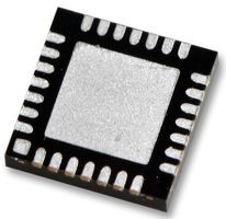
1:4 LVDS low-jitter clock buffer with single-ended input, operating at frequencies up to 350MHz. This integrated circuit features four LVDS outputs, a 1.71V to 3.63V supply voltage range, and a maximum supply current of 10mA. Packaged in a compact QFN format with dimensions of 4mm x 4mm x 0.85mm, it offers a propagation delay of 4ns and a turn-on delay time of 2.5ns. The device supports a duty cycle up to 60% and operates within a temperature range of -40°C to 85°C, adhering to RoHS compliance.
Checking distributor stock and pricing after the page loads.
Sign in to ask questions about the Silicon Labs Si5330L-B00228-GM datasheet using AI. Get instant answers about specifications, features, and technical details, ideal for finding information in larger documents.
Sign In to ChatWidest selection of semiconductors and electronic components in stock and ready to ship ™
Silicon Labs Si5330L-B00228-GM technical specifications.
| Package/Case | QFN |
| Duty Cycle | 60% |
| Frequency | 350MHz |
| Height | 0.85mm |
| Input | LVTTL |
| Length | 4mm |
| Logic Function | Clock |
| Max Duty Cycle | 60% |
| Max Frequency | 350MHz |
| Max Operating Temperature | 85°C |
| Min Operating Temperature | -40°C |
| Max Supply Voltage | 3.63V |
| Min Supply Voltage | 1.71V |
| Number of Circuits | 1 |
| Number of Outputs | 4 |
| Package Quantity | 75 |
| Packaging | Tray |
| Propagation Delay | 4ns |
| Reach SVHC Compliant | Unknown |
| RoHS Compliant | Yes |
| Series | SI5330L |
| Supply Current | 10mA |
| Turn-On Delay Time | 2.5ns |
| Width | 4mm |
| RoHS | Compliant |
Download the complete datasheet for Silicon Labs Si5330L-B00228-GM to view detailed technical specifications.
The embedded preview will load automatically when this section scrolls into view.
